Micron Ships World’s First 232-Layer NAND
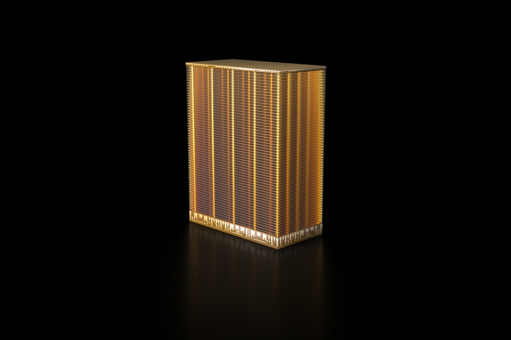
Micron Technology has announced that it has begun volume production of the world’s first 232-layer NAND, built with industry-leading innovations to drive unprecedented performance for storage solutions. It features the industry’s highest areal density and delivers higher capacity and improved energy efficiency over previous generations of Micron NAND, to enable best-in-class support of the most data-intensive use cases from client to cloud.
“Micron’s 232-layer NAND is a watershed moment for storage innovation as first proof of the capability to scale 3D NAND to more than 200 layers in production,” said Scott DeBoer, executive vice president of technology and products at Micron. “This groundbreaking technology required extensive innovation, including advanced process capabilities to create high aspect ratio structures, novel materials advancements and leading-edge design enhancements that build on our market-leading 176-layer NAND technology.”
As the world generates more data, customers must expand their storage capacity and performance while reducing energy consumption and meeting more stringent environmental sustainability requirements. Micron’s 232-layer NAND technology provides the high-performance storage necessary to support advanced solutions and real-time services required in data center and automotive applications, as well as responsive, immersive experiences on mobile devices, consumer electronics and PCs. This technology node enables the introduction of the industry’s fastest NAND I/O speed ‒ 2.4 gigabytes per second (GB/s) ‒ to meet the low-latency and high-throughput needs of data-centric workloads such as artificial intelligence and machine learning, unstructured databases and real-time analytics, and cloud computing.1 That speed represents a 50% faster data transfer than the fastest interface enabled on Micron’s 176-layer node.2 Micron 232-layer NAND also delivers up to 100% higher write bandwidth and more than 75% higher read bandwidth per die than the prior generation.2 These per-die benefits translate to performance and energy efficiency gains in SSDs and embedded NAND solutions.
In addition, 232-layer NAND introduces the world’s first six-plane TLC production NAND.3 It has the most planes per die of any TLC flash3 and features independent read capability in each plane. The combination of high I/O speed, read and write latency, and Micron’s six-plane architecture provides best-in-class data transfers in many configurations. This structure ensures fewer collisions between write and read commands and drives system-level quality-of-service improvements.
Micron’s 232-layer NAND is the first in production to enable NV-LPDDR4, a low-voltage interface that delivers per-bit transfer savings of more than 30% compared to prior I/O interfaces. As a result, 232-layer NAND solutions offer ideal support for mobile applications and deployments in the data center and at the intelligent edge that must balance improved performance with low power consumption. The interface is also backward compatible to support legacy controllers and systems.
The compact form factor of 232-layer NAND offers customers flexibility in their designs while enabling the highest TLC density per square millimeter ever produced (at 14.6 Gb/mm2).3 The areal density is between 35% and 100% greater than competing TLC products in the market today.3 Shipping in a new 11.5mm x 13.5mm package, 232-layer NAND features a 28% smaller package size than previous Micron generations,2 making it the smallest high-density NAND available.3 More density in a smaller footprint minimizes board space for a diverse set of deployments.
Next-Generation NAND Enables Innovation Across Markets
“Micron has sustained technology leadership with successive first-to-market advancements in NAND layer count that enable benefits like longer battery life and more compact storage for mobile devices, better performance in cloud computing, and faster training of AI models,” said Sumit Sadana, chief business officer at Micron. “Our 232-layer NAND is the new foundation and standard for end-to-end storage innovation underpinning digital transformation across industries.”
The development of 232-layer NAND is the result of Micron’s leadership in research, development and process technology advancements. The breakthrough capabilities of this NAND will enable customers to deliver more innovative solutions in data centers, thinner and lighter laptops, the latest mobile devices and across the intelligent edge.
Availability
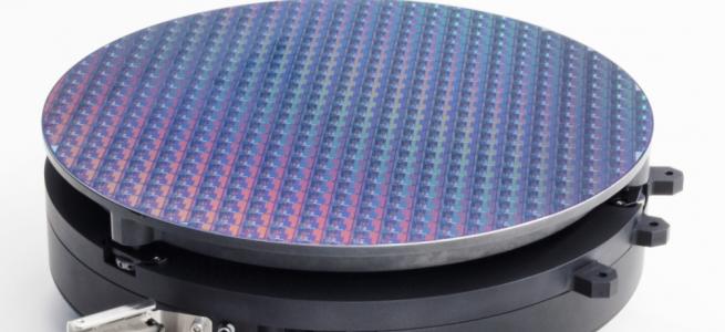
Micron’s 232-layer NAND is now in volume production in the company’s Singapore fab. It is initially shipping to customers in component form and through its Crucial SSD consumer product line. Additional product and availability announcements will follow.
Micron's NAND Center of Excellence in Singapore is recognized by the World Economic Forum’s Global Lighthouse Network for operational excellence in smart manufacturing. Advancements including AI tools, smart control systems and predictive capabilities allow Micron to accelerate product development, improve quality and achieve faster manufacturing yield ramps to shorten the time to market.