Failure Analysis and Reliability Testing: Why SAM is Now Considered Essential Equipment
Scanning Acoustic Microscopy (SAM) has become integral testing equipment in semiconductor supply chain integrity, inline manufacturing, R&D, quality control labs, and even for 100% inspection of all manufactured materials
In manufacturer test labs, R&D centers, material research groups, and quality control departments, the search for minute defects is spurring investment in Scanning Acoustic Microscopy (SAM) equipment. The failure analysis and reliability detection metrology technology has become essential and is now taking its place alongside other lab testing and measurement instrumentation like X-ray and scanning electron microscopes (SEM). In current market conditions with electronics supply chain extremely constrained, SAM is a highly effective tool to help mitigate proliferation of counterfeit components in semiconductor supply chain.
SAM, also known as Ultrasonic Non-Destructive Testing (NDT), is utilized in industry to identify small defects in products or components during manufacturing and to analyze the specific root cause of a failure when a device fails in the field. The demand for this kind robust failure detection capability is increasing the technology’s use among manufacturers of consumer, industrial, and military electronic devices.
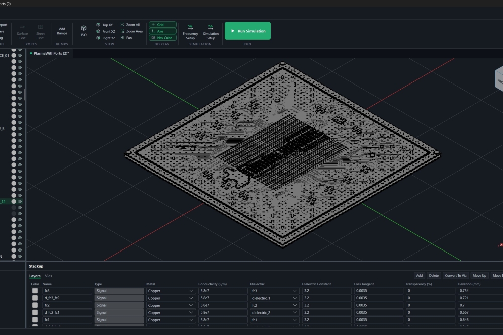
SAM offers powerful non-invasive, non-destructive imaging and materials analysis for inspecting the internal structures of opaque materials. Depth-specific information can be extracted and applied to create two-and three-dimensional images without time-consuming tomographic scan procedures or costly X-ray equipment. Specialists can analyze SAM images to detect and characterize device flaws such as cracks, delamination, inclusions and voids in bonding interfaces as well as evaluate soldering and other interface connections on PCBs.
Recent advances in SAM facilitate the detection of much smaller defects than previously possible.
“Advanced, phased array SAM systems make it possible to move to a higher level of failure analysis because of the level of detection and precision involved. In the past, detecting a 500-micron defect was the goal; now it is a 50-micron defect. With this type of testing, we can inspect materials and discover flaws that were previously undetected,” said Hari Polu, President of OKOS, a Virginia-based manufacturer of industrial SAM ultrasonic non-destructive testing systems. The company serves the electronics manufacturing, aerospace, and metal/alloy/composite manufacturers, and end-user markets.
When manufacturers take advantage of the higher level of failure detection and analysis, the production yield and overall reliability of electronic devices improve significantly. Projects are expedited and potential points of failure are eliminated in the field.
Because of the significant benefits of utilizing SAM, a growing number of manufacturers are equipping R&D and QA labs with the metrology equipment, as well as integrating it into production lines for 100% inspection.
Semiconductors and Electronics
In the semiconductor and electronics industries, the need for non-destructive failure analysis and reliability testing is accelerating. In these sectors, manufacturing with extreme consistency without defects or impurities is essential. This is the case whether the products are wafers, discrete electronics, or the packaged assemblies used in phones, video games, EV automobile sub-systems, or rocket sub-systems.
SAM addresses this need of the semiconductor and electronics industries. The testing is already the industry standard for 100% inspection of semiconductor components to identify defects such as voids, cracks, and the delamination of different layers within microelectronic devices.
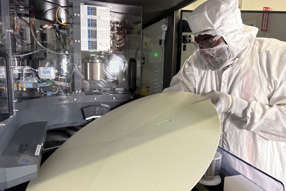
Beyond the semiconductor components themselves, today’s electronics products contain various specialty metals, alloys, plastics, and glass components. All semiconductor components need to be enclosed and packaged in consumer usable form factors. As a result, SAM equipment has evolved and is now being used to detect subsurface flaws, dis-bonds, cracks, and other irregularities in these types of materials that constitute the “packaging” of semiconductor components.
Due to the critical nature of many of the components made from these materials, high purity alloys should be highly consistent, with extremely low levels of impurities and contaminations. High purity metals and alloys such as aluminum, zinc, cobalt, copper, titanium, zirconium, molybdenum, magnesium, and stainless steel are the backbone of many industries, from electronics to aerospace, and medical devices.
Scanning Acoustic Microscopy
Scanning acoustic microscopy functions by directing focused sound from a transducer at a small point on a target object. The sound hitting the object is either scattered, absorbed, reflected, or transmitted. By detecting the direction of scattered pulses as well as the “time of flight,” the presence of a boundary or object can be determined as well as its distance.
To produce an image, samples are scanned point by point and line by line. Scanning modes range from single layer views to tray scans and cross-sections. Multi-layer scans can include up to 50 independent layers. Depth-specific information can be extracted and applied to create two-and three-dimensional images without the need for time-consuming tomographic scan procedures or costly X-ray equipment. The images are then analyzed to detect and characterize flaws such as cracks, inclusions, and voids.
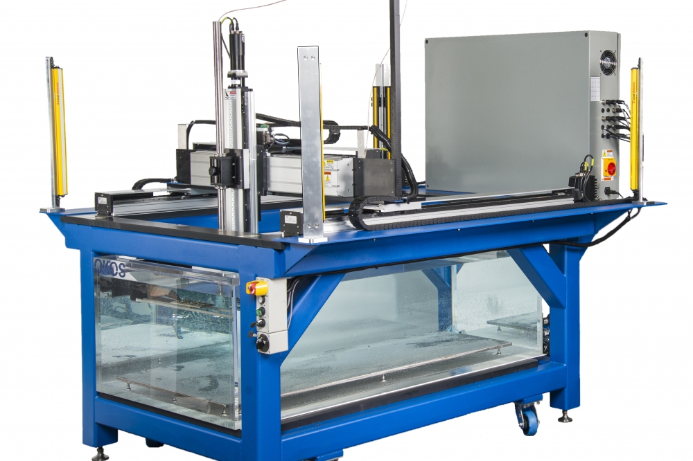
Smaller manufacturers and independent testing labs are likely to have a tabletop SAM model that provides a scan envelope of over 300 mm with a maximum scan velocity of 500 mm/s and accuracy and repeatability of +/- 5.0 micron. Software allows using saved data to virtually re-scan, view, and analyze data for simultaneous real-time analysis or post collection review. Often, such tabletop units are used to analyze data for failure analysis, product inspection, quality control, R&D, process validation, as well as to determine product reliability, in process quality control, and vendor qualification.
As requirements rise to accommodate testing for higher levels of production, manufacturers will often utilize a larger system with the capability of high speed inspection. The challenge, however, is to perform this inspection at extremely high throughput with 100% inspection to identify and remove components that do not meet quality requirements. This necessitates more advanced equipment that can simultaneously inspect several layers, often on multiple channels, scanning multiple samples in handling trays in an automated fashion to accelerate the process.
According to Polu, SAM can also be custom designed to be fully integrated into high volume manufacturing systems. Advanced, phased array systems detect minute flaws in specialty metals and alloys for 100% inspection of all materials. Semiconductor fabs now have access to 100% inspection of wafers, panels, and singulated components in trays.
Fortunately, recent advancements in SAM technology have significantly improved throughput speeds and defect detectability. When high throughput is required for 100% inspection, ultra-fast single or dual gantry scanning systems are utilized along with 128 sensors for phased array scanning. Multiple transducers can also be used to simultaneously scan for higher throughput.
“A conventional 5 MHz sensor could take up to 45 minutes to inspect an 8–10-inch square or disc alloy. Today, however, an advanced phased array with 64-128 sensors and innovative software to render the images can reduce inspection time to five minutes, with more granular detection of small impurities or defects,” says Polu.
As important as the physical and mechanical aspects of conducting a scan, the software is critical to improving the resolution and analyzing the information to produce detailed scans.
Multi-axis scan options enable A, B, and C-scans, contour following, off-line analysis, and virtual rescanning for composites, metals, and alloys. This results in highly accurate internal and external inspection for defects and thickness measurement via the inspection software.
Various software modes can be simple and user friendly, advanced for detailed analysis, or automated for production scanning. An off-line analysis mode is also available for virtual scanning.
Polu estimates that OKOS’ software-driven model enables them to drive down the costs of SAM testing while delivering the same quality of inspection results. Consequently, this type of equipment is well within reach of even modest testing labs.
“Every company will eventually move towards a higher level of failure analysis because of the stringent detection and precision requirements today,” says Polu. “The cost advantages and time savings of industrial SAM equipment make this possible.”
With labs in Santa Clara, CA, Phoenix, AZ and Manassas, VA, OKOS offers contract analysis and testing services that meet existing industrial and military standards. The service also provides customers the ability to vet technology and feasibility prior to investing in equipment.
Today, across a range of industries, SAM offers the best value due to the exceptional level of failure analysis detail it provides, compared to conventional methods. As a result, advanced SAM systems are now considered essential tools in R&D and Quality Assurance labs, as well as high speed production lines.