Tiny Chip-Based Device Performs Ultrafast X-Ray Manipulation
Optical microelectromechanical systems (MEMS) are tiny microchip-size devices that control light and communications. Separately, time-resolved X-ray probes are devices that help scientists study highly transient phenomena. These phenomena are short-lived and involve fast structural and functional changes. Scientists have now developed X-ray optics based on specially designed and fabricated MEMS that can harness extremely short X-ray pulses. The new devices are much smaller and lighter than conventional devices used to operate X-ray probes, and they could be essential for experiments on ultrafast phenomena at synchrotron and free-electron laser X-ray sources.
The new ultrafast optics-on-a-chip device will be orders of magnitude smaller and lighter than conventional devices used to manipulate X-ray probes. This will enable innovative X-ray research and applications. The device could help scientists study fast-evolving chemical, material, and biological processes. The results could aid in the development of efficient solar cells and batteries, advanced computer storage, and novel drugs. In this study, scientists demonstrated the device at a synchrotron facility. A fully developed version could be used with the X-ray generators found in hospitals and university laboratories. In these settings, the devices could support fast non-destructive diagnostics or precise dosage for radiation therapy.
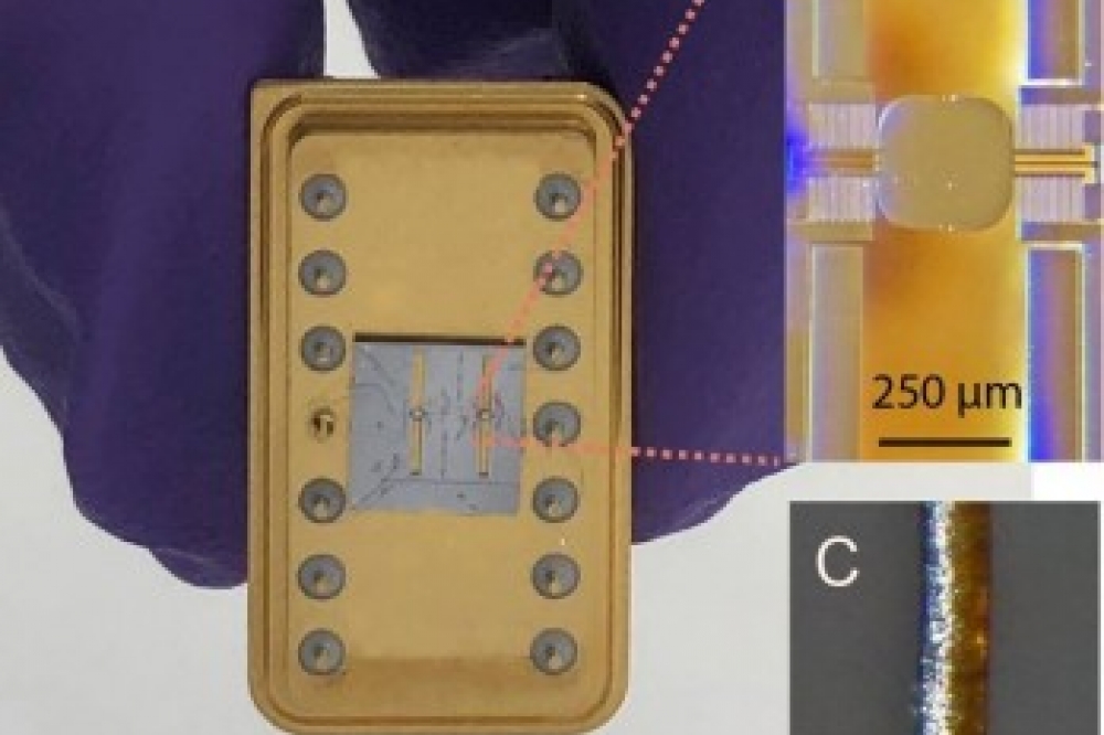
The research team, consisting of scientists from the Advanced Photon Source (APS) and Center for Nanoscale Materials (CNM), demonstrated the X-ray optics-on-a-chip device using the X-ray source at the APS. The APS and CNM are Department of Energy (DOE) scientific user facilities at Argonne National Laboratory. The device, designed at the CNM, measures only 250 micrometers and weighs just 3.5 micrograms. The extremely small size and low weight of the MEMS-based shutter allow it to oscillate at speeds equivalent to about one million revolutions per minute. The researchers leveraged this high speed and the MEMS material’s X-ray diffractive property to create an extremely fast X-ray shutter. The resulting ultrafast X-ray optics-on-a-chip can manipulate hard X-ray pulses exceeding 350 MHz, or 1,000 times higher than any mechanical modulator. Moreover, the devices' timing characteristics can be tuned for a host of dynamic X-ray instruments and applications, impossible with traditional optics that are typically one billion times more massive. The X-ray optics-on-a-chip devices set the stage for future dynamic and miniature X-ray optics for time-domain science and accelerator diagnostics and control, including wave-front manipulation, spectral dispersion, multiplexing, and pulse slicing.
The research was supported by DOE’s Office of Science, Basic Energy Sciences, Scientific User Facilities Division.