EV GROUP expands collaboration with ITRI
EV Group (EVG), a supplier of wafer bonding and lithography equipment for the MEMS, nanotechnology and semiconductor markets, has announced that it has expanded its collaboration with the Industrial Technology Research Institute (ITRI), one of the world’s leading applied technology research institutes based in Hsinchu, Taiwan, on developing advanced heterogeneous integration processes.
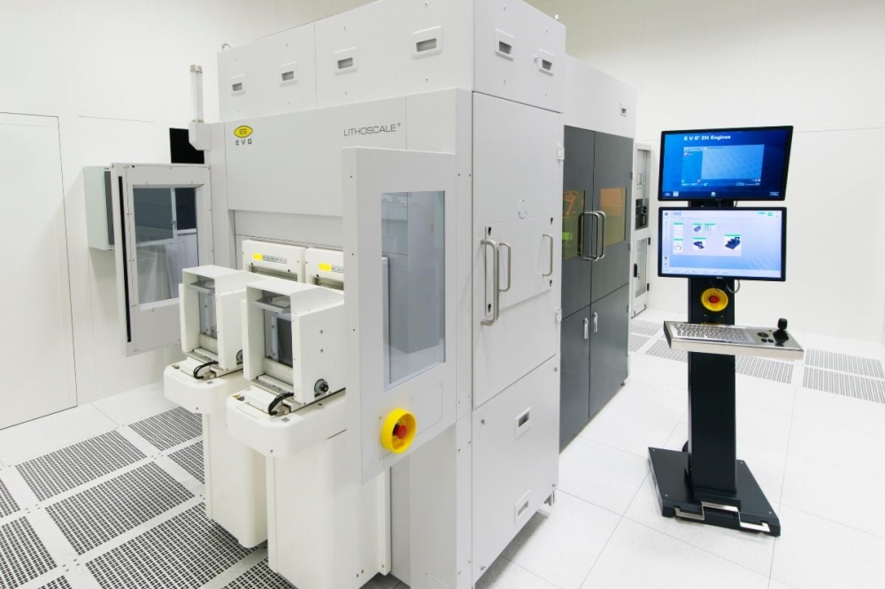
With the support of the Department of Industrial Technology (DoIT) of the Ministry of Economic Affairs (MOEA), Taiwan, ITRI established the Heterogeneous Integration Chip-let System Package Alliance (Hi-CHIP) to help create an ecosystem covering package design, testing and verification, and pilot production, to achieve the goal of supply chain localization and expand business opportunities. As a member of the Hi-CHIP Alliance, EVG has provided several of its most advanced wafer bonding and lithography systems, including the LITHOSCALE® maskless exposure lithography system, EVG®850 DB automated debonding system, and GEMINI®FB hybrid bonding system. The installation of these high-volume-manufacturing platforms at ITRI’s state-of-the-art facility will help enable EVG’s and ITRI’s shared customers to accelerate the development and transfer of new heterogeneous integration processes from R&D to customers’ fabs.
In semiconductor manufacturing, 3D vertical stacking and heterogeneous integration – the manufacturing, assembly and packaging of multiple different components and dies into a single device or package – are increasingly important for higher performance beyond transistor scaling. 3D and heterogeneous integration are enabling high-bandwidth interconnects in advanced packaging to achieve overall system performance gains, and thus have become a crucial driver for artificial intelligence (AI), autonomous driving and other high-performance computing applications. As a result, the MOEA is proactively following up and bridging the resources with national-scale R&D projects such as “AI Chip Heterogeneous Integrated Module Advanced Manufacturing Platform” and “Programmable Heterogeneous 3D Integration”.

| ITRI Headquarters, Chutung, Hsinchu County, Taiwan. Source: ITRI. |
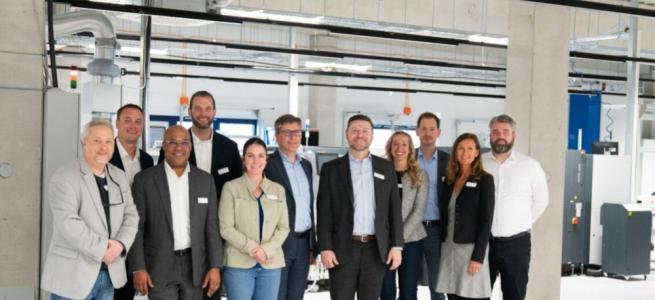
“Key to our Triple-i philosophy of invent-innovate-implement is our focus on engaging with world-leading research institutes, like ITRI, to accelerate the development and commercialization of new technologies that drive future innovations in the semiconductor industry,” stated Hermann Waltl, executive sales and customer support director and member of the executive board at EV Group. “Our ongoing collaboration with ITRI gives us access to world-class research expertise and further enhances our process support infrastructure in Taiwan, which EVG has significantly expanded over the years to better meet the growing needs and challenges that our customers and partners in the region face. This includes our exceptional process and application engineering team based in multiple locations across Taiwan, which complements the services provided at EVG’s Heterogeneous Integration Competence Center at our headquarters in Austria.”

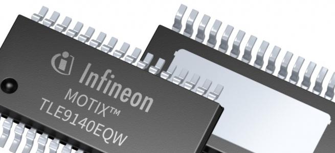
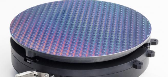
The LITHOSCALE® maskless exposure lithography system from EV Group is one of several tools providing revolutionary process solutions to the Chip-let System Package Alliance (Hi-CHIP) led by ITRI. Source: EV Group.