Henkel unveils semiconductor CIF for advanced silicon node flip chip applications

Henkel has announced the commercialization of its latest semiconductor-grade capillary underfill (CUF) formulation for advanced packaging applications. The material, Loctite Eccobond UF 9000AG, enables advanced silicon (Si) node flip chip integration by providing robust interconnect protection and compatibility with high-volume manufacturing environments. While the company has well-established pre-applied paste and film underfill materials for leading-edge chip technologies, this development broadens Henkel’s post-applied capillary portfolio for flip chips with advanced node scaling.
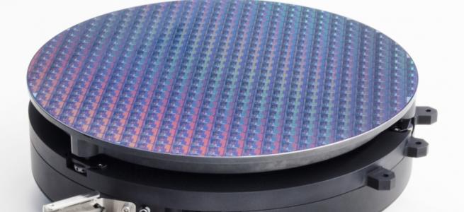
Loctite Eccobond UF 9000AG breaks past conventional formulation paradigms, balancing high filler loading and fast flow capability to meet the extreme reliability and volume demands of next-generation semiconductor device packaging. Already proven in mass production environments with the latest node and currently under evaluation for next-generation node flip chip packages, the product is an epoxy-based underfill designed with a high glass transition temperature (Tg) and ultra-low (<20 ppm) coefficient of thermal expansion (CTE). Though among the market’s highest filled (>70%) formulations to enable excellent bump protection, it still underfills 30% faster as tested against previous-generation and competitive CUFs. In addition, Loctite Eccobond UF 9000AG provides high fracture toughness, low warpage, and MSL3 reliability on dies ranging in size from 10mm x 10mm to 20mm x 20mm.
“This innovative solution represents a major breakthrough for the future of advanced node flip chip device processing and end product performance,” said Ramachandran Trichur, Henkel’s Global Market Segment Head for Semiconductor Packaging Materials, explaining the significance of the material’s unique filler, resin and hardener balance. “Historically, high filler loading has correlated with slower underfilling rates. Loctite Eccobond UF 9000AG moves beyond this boundary. It gives integrators of the latest node – and potentially next-generation node – chips a more comprehensive low CTE, high flow solution that marries productivity and thorough solder joint protection.”
The increasing use of the latest node flip chips and the projections that next-generation node scaling devices will be in volume production by year’s end underscore the immediate requirement for a proven, reliability-enhancing chip protection solution. Loctite Eccobond UF 9000AG meets the challenging performance metrics of advanced mobile devices and, having passed harsher thermal cycling level C testing (-65° C to 150° C), may also be a good candidate for certain automotive electronic and computing applications.