Okmetic Expands RFSi® Portfolio
Okmetic’s Engineered Ultra High Resistivity wafer is a close to zero -loss silicon wafer dedicated for RF filter devices. The wafer combines over 10 kOhm-cm resistivity, low Oi and highly efficient, purely silicon-based, trap-rich layer.
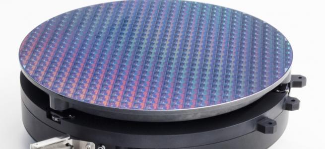
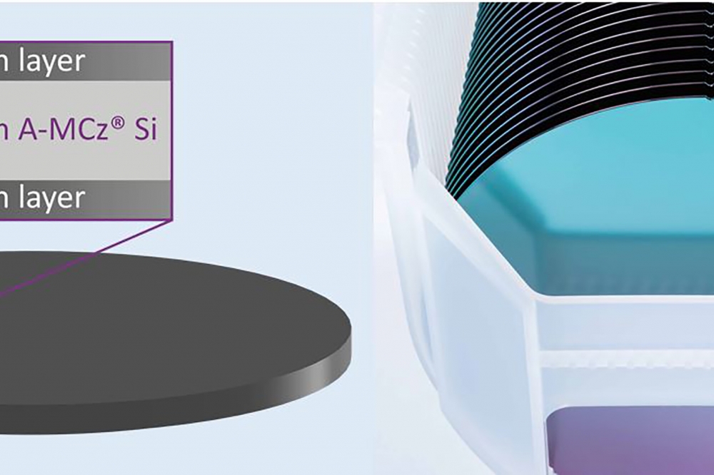
Okmetic, the supplier of advanced silicon wafers for the manufacture of MEMS, sensor, RF and power devices, has announced the release of Engineered Ultra High Resistivity wafer, a premium silicon substrate dedicated for demanding RF filters and devices. This highly advanced wafer technology leverages Okmetic’s proprietary A-MCzÒ crystal growth process to deliver the highest resistivity and best technical performance in the form of close to zero substrate-induced losses and nonlinearities for RF devices. Also, Okmetic Ultra High Resistivity wafers’ oxygen content is optimized, which improves wafer strength and makes them a viable option for ultra high resistivity FZ wafers.
The Engineered Ultra High Resistivity wafer is an expansion to Okmetic’s highly popular portfolio of high resistivity RFSi® wafers. Okmetic has delivered over 2 million high resistivity RFSi® wafers to the leading RF manufacturers and rapidly gained a significant share in the market. The demand for engineered high resistivity wafer solutions is expected to continue strong, and this new wafer launch will be catering for the high-end substrate needs of RF device manufacturers.
“Okmetic is extremely proud to introduce the new Engineered Ultra High Resistivity wafer boasting over 10,000 Ohm-cm of bulk resistivities, low Oi and highly efficient trap-rich layer. This is a premium silicon substrate enabling maximum performance and stable resistivity along with close to zero substrate-induced losses and nonlinearities for RF devices", says Atte Haapalinna, Chief Technology Officer at Okmetic. “We are very pleased to be able to respond to the most demanding substrate needs that our RF customers have expressed. The Engineered Ultra High Resistivity wafer is the result of long-term development work and true demonstration of Okmetic’s exceptional crystal growth expertise and its capability of taking doping process to extremes.”
Engineered Ultra High Resistivity wafers enable RF filters to reach very low second harmonic levels of < -90 dBm measured at 900 MHz fundamental tone, and extremely low IMD3 levels of even < -105 dBm. More information of the results on Okmetic website.
Availability
Engineered Ultra High Resistivity wafers are offered in 200 millimeter diameter and in volumes initially in <100> orientation. 200 mm Engineered Ultra High Resistivity wafers in <111> orientation are ready for sampling. These wafers include UF-RFSi® (Ultra Flat High Resistivity wafer with trap-rich layer) and wafers for GaN-on-Si applications in RF (without trap-rich layer). Sample shipment order intake will begin upon launch of the wafer. For sales information and custom quotes, please contact your regional sales representative