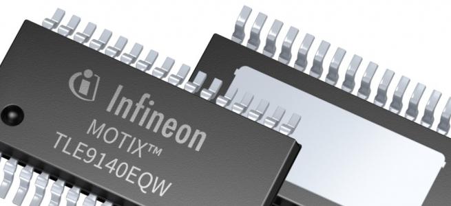
EV GROUP and Toppan Photomask join forces

EV Group (EVG), a leading supplier of wafer bonding and lithography equipment for the MEMS, nanotechnology and semiconductor markets, and Toppan Photomask Co. Ltd., the world’s premier photomask provider, today announced that they have entered into an agreement to jointly market nanoimprint lithography (NIL) as an enabling high-volume manufacturing (HVM) process for the photonics industry.
The collaboration, which combines the strengths of the leading supplier and pioneer of NIL systems and the leading supplier of photomasks to the semiconductor market, aims to establish NIL as an industry standard production process for photonics manufacturing, and accelerate its implementation in HVM to support a wide variety of applications. These applications include augmented/mixed/virtual reality headsets, smartphone and automotive sensors, as well as medical imaging systems.

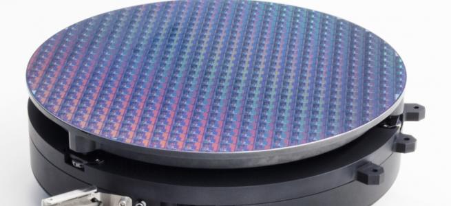
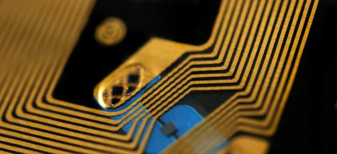
Process engineers at EV Group’s NILPhotonics® Competence Center examine a 200-mm wafer with metalenses replicated using a master manufactured by Toppan Photomask and a nanoimprint lithography (NIL) process from EVG. Source: EV Group.
As part of this non-exclusive collaboration, EVG and Toppan Photomask will pool their knowledge, expertise and services to provide NIL development kits utilizing master templates from Toppan Photomask and equipment and process development services provided by EVG to further promote NIL technology and its possibilities for industrial-scale implementation. In addition, EVG will offer NIL technology and product demonstrations to interested companies at EVG’s NILPhotonics® Competence Center at its headquarters in Austria. Furthermore, each company will designate the other as a recommended supply chain partner to companies interested in leveraging NIL to support their production needs.
“Toppan Photomask is very excited to enter into a collaboration with EVG”, said Chan-Uk Jeon, chief technology officer of Toppan Photomask Co., Ltd. “EVG’s NIL tooling and processing capabilities are world class and will enable cost-effective growth in photonics and other new technologies that are now adapting to NIL technology. Toppan Photomask sees a bright future as NIL grows into another successful lithography solution, enabled by both companies’ established strengths.”

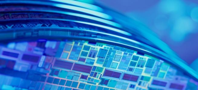
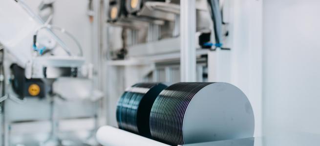
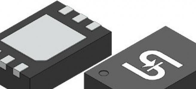
Toppan Photomask manufactures photomasks for the semiconductor industry like the one shown here. Nanoimprint lithography (NIL) masters are made using the same materials, technology and techniques. Source: Toppan Photomask.
Bringing Nanoimprint Lithography to Mainstream Manufacturing
Traditional lithography technologies are reaching their limits when it comes to addressing future applications that require the creation of small and arbitrarily shaped patterns, such as metalenses. NIL is a proven, cost-effective process for generating nanometer-scale-resolution patterns on complex structures, and thus is a viable alternative for these applications. NIL can replicate these complex structures very efficiently, on large areas, with fewer design constraints and a very streamlined process flow, for both prototyping and HVM.
EVG has been a pioneer in NIL technology for more than 20 years and has helped to foster a wider NIL ecosystem through partnerships across the NIL supply chain – from suppliers of optical materials (such as adhesives and resists), substrate materials and stamp production to optical component and device manufacturers. With this collaboration between two established industry leaders in lithography and photomask fabrication, respectively, EVG and Toppan Photomask intend to fuel the adoption of NIL as a mainstream HVM technology for the photonics industry.
According to Markus Wimplinger, corporate technology development and IP director at EV Group, “We are excited to be partnering with Toppan Photomask to bring nanoimprint lithography to mainstream manufacturing applications. As the leading supplier of semiconductor photomasks with a reputation for the highest-quality standards, Toppan Photomask has extensive experience working with standardized production methods involving the world’s most stringent manufacturing requirements. This first-of-its-kind collaboration between a nanoimprint process equipment and services provider and a nanoimprint master manufacturer is a huge win for the industry and will aid our customers in quickly scaling up NIL as a mass-production technology for advanced optical devices and components – helping them to bring new ‘virtual’ ideas into reality.”
Upcoming Nanoimprint Industry Events
Experts from both companies will be available to discuss this collaboration at the Micro and Nano Engineering (MNE) Eurosensors 2022 Conference, taking place at the Gasthuisberg academic campus in Leuven, Belgium, from September 19-23. Event attendees can visit EVG at Booth #S8 to learn more.
In addition, Christine Thanner of EVG is giving an invited plenary talk at the Nanoimprint and Nanoprint Technology (NNT) Conference in Toyama, Japan on October 5, titled “Nanoimprint – from niche to high-volume manufacturing,” where she will address the importance of having a matching combination of NIL mastering techniques, replication equipment and processes.
NILPhotonics Competence Center: A Flexible Cooperation Model
EVG’s NILPhotonics Competence Center provides an open access innovation incubator for customers and partners across the NIL supply chain to collaborate to shorten development cycles and time to market for innovative photonic devices and applications. The center is highly flexible and adapts to the varied needs of customers while ensuring the highest level of IP protection for every aspect of development. The cleanroom is designed to meet the most stringent customer requirements and allows for virtual line concepts where wafers are reintroduced into customer fabs for further processing. More information is available at https://www.evgroup.com/products/process-services/nilphotonics-competence-center/.