New Brewer Science bonding & dielectric materials deliver packaging solutions for 5G, IoT devices

Semiconductor IC packaging techniques include the
utilization of 3D integration to increase chip density, maximize performance
and reduce power consumption. Brewer Science, a global technology leader in the
development and manufacturing of innovative materials and processes, has
introduced its latest packaging solutions utilizing a permanent bonding
material and a photo-imageable dielectric for the fabrication of cutting-edge
semiconductors as well
as 5G and IoT microelectronic devices.
By Baron Huang, Mei Dong, and Ziwei Liu, Brewer Science
Permanent
Bonding Material with High Thermal Budget
Bonding two components together permanently is applied in
many fields of advanced packaging to offer a
z-axis direction of integration for the fabrication of three-dimensional
integrated circuits (3D ICs). Such permanent bonding techniques include
direct/fusion bonding, anodic bonding, soldering, and thermocompression. While
fusion bonding is still the most frequently used permanent bonding technology
in today’s semiconductor industry, there is a fast-growing trend for adhesive
bonding.
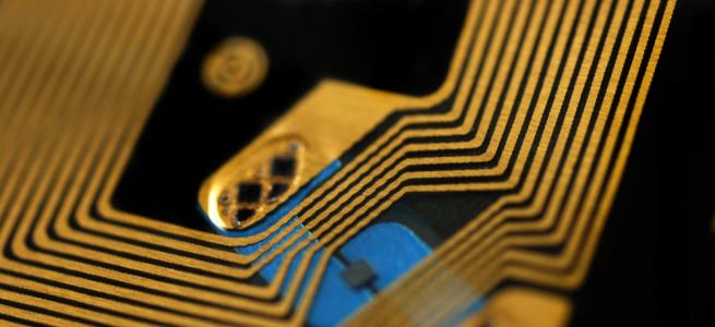
Adhesive bonding, which develops a bond connecting one surface to another using a polymeric material as the intermediate layer, brings significant advantages including: 1) improved design flexibility; 2) good surface planarization and adaptability to surface topography; 3) lower bonding temperature for protecting sensitive components; and 4) better tolerance to particles. With all these merits, adhesive bonding has recently received much attention for microelectromechanical systems (MEMS) packaging and heterogeneous integration to assemble individual IC components such as logic chips, memory chips, and image sensor devices together into high-density, ultra-thin integrated packages. Such modules are needed for high-performance computing applications such as artificial intelligence (AI), data centers, 5G, and high-end mobile products.
Brewer Science previously introduced its first permanent bonding adhesive, the PermaSOL® family of materials, at the European 3D & Systems Summit. PermaSOL materials were designed to address chip-level and wafer-level packaging requirements by providing reliable bonds with good thermal stability and with low moisture absorption. Brewer Science is now introducing its next generation of permanent bonding materials (PBM) with excellent thermal stability and an improved thermal budget up to 350°C. These materials further provide room temperature bonding with low pressure, low dielectric constant, high chemical resistance, and long shelf life.
In comparison to benzocyclobutene, a widely used bonding adhesive, the Brewer Science next generation PBM exhibits even lower curing temperature, smaller tensile strength and modulus, and larger CTE. These characteristics make the Brewer Science material a ‘super low-stress resin’ providing the benefits of low warpage, which brings up promising opportunities for applications on flexible substrates.
Next generation PBM exhibits
good thermal stability with a decomposition temperature above 470°C in a
nitrogen atmosphere. The bonding can be achieved at 25°C, 2 kN, for 2 minutes,
due to the intrinsic flexibility and fluidity of the material.

Figure 1. C-SAM images of next
generation PBM after bonding at room temperature (left), after thermal testing
at 300 °C for 1 hour (center), and after thermal testing at 350 °C for 1 hour
(right)
Figure 1 shows the bonding quality of the next generation PBM characterized by a SONIX Scanning Acoustic Microscope, demonstrating a void-free bondline. After bonding, the adhesive material is solidified via a thermal curing process. The material starts to cure at 160°C. Over 90 percent curing is realized when cured at 250°C for 3 minutes or 220°C for 30 minutes. A high temperature (300°C and 350°C) thermal test was also conducted on the cured material to further investigate its thermal stability. The C-SAM images in Figure 1 shows that next generation PBM has a good thermal budget: defect-free and low shrinkage after heat treatments at 300°C and 350°C for one hour.
Low-loss photo-imageable
dielectric
With the exploding demand for high-rate data connectivity, new spectrum
for 5G mobile networks is being rapidly deployed worldwide. Since 2019, service
providers have initiated a race for the 5G market—put another way: the
fifth-generation technology standard for broadband cellular networks. Many
network operators subsequently reported realizing the fascinating capabilities
of 5G, including superior speeds and low latencies, which quickly expanded the
number of use cases and further boosts the demand for data and performance.
In this 5G era, there is a growing demand for new materials and new packaging architectures to ensure low signal loss for high bandwidth millimeter wave (mmWave) RF transmission. Also needed is reliable measurements, especially in wafer level packaging, 3D integration, TSV filling, and stress-buffering applications. The 5G spectrum utilizes higher frequencies, which can lead to a greater risk of signal loss.
Photo-imageable dielectric (PID) with low-loss is now in the spotlight, especially for high-speed and high-frequency applications. Various polymeric dielectric materials have been evaluated as PID for packaging high-speed and high-frequency devices, including polybenzoxazole, polyimide, polysiloxane, and epoxy/phenol. However, most of them show a dielectric constant greater than three and with a dissipation factor of around 0.02, which might be fine for the existing applications with frequencies in the sub-6 GHz bands, but cannot meet the requirement and future challenges to be found with frequencies at 60 GHz or beyond for 5G mmWave communication.
Herein, Brewer Science has developed a new low-loss PID material to meet the growing demand for 5G mmWave and IoT applications. The dielectric constant (Dk) for the Brewer Science low-loss PID material is measured to be 2.6 at 10 GHz and at 108 GHz, while the dissipation factor (Df) is 0.0016 at 10 GHz and 0.0041 at 108 GHz. Furthermore, the low-loss PID material can be patterned at low UV exposure dosages, around 300 mJ/cm2; it provides good line/space resolution with an aspect ratio around 1:1; patterned line/space, trench, and via features are shown in Figure 2. A steep sidewall angle close to 90 degrees that is free of footing/rounding is also observed in SEM/FIB images of the low-loss PID material.

Figure 2. SEM/FIB images of (a)
low-loss PID material on silicon substrate; (b) low-loss PID material on Ti/Cu
substrate
Besides the need for a low dielectric constant and loss tangent, additional requirements for the photo-imageable dielectric include strong adhesion, good thermal stability and reliability as well as low moisture uptake, high elongation, low shrinkage, and high photosensitivity. The adhesion quality for the Brewer Science low-loss PID material was examined by crosshatch tape peel testing.

Figure 3. Cross hatch tape peel
testing suggests good adhesion of low-loss PID material to various substrates,
including Si, Glass, Al, and Ti/Cu surfaces
Figure 3 shows the low-loss PID
has a good adhesion (4B) to various substrates, including silicon, glass and
aluminum as well as titanium and copper surfaces. Other properties of the
low-loss PID material are summarized in table 1, which shows the material can
meet or even exceed the demands for a wide range of applications for the
packaging of high-speed and high-frequency devices.

Table 1. Properties of Brewer
Science’s next generation PBM and low-loss PID materials
Summary
This paper introduces a newly
developed permanent bonding material (PBM) and a low-loss photo-imageable
dielectric (low-loss PID) from Brewer Science. Its general material properties
are summarized in Table 1. These materials offer many benefits
including excellent thermal stability, low bonding temperature and
pressure as well as low Dk and Df in addition to strong adhesion to various
substrates. These many beneficial qualities make them attractive candidates to
meet the growing demand for 5G and IoT device packaging where reliability,
efficiency, and performance are critical to success.