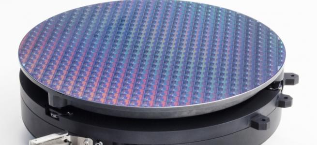
Onto Innovation’s ‘XL’ fine resolution large field lithography dramatically cuts FOPLP pattern distortion

Heterogeneous integration enables multiple chips from varying Silicon processes to deliver superior performance. In large panel packages, present day limits on exposure field size forces manufacturers to ‘stitch’ together multiple reticles, which slows throughput and increases costs. Onto Innovation’s new JetStep® X500 system dramatically increases the exposure field up to 250 x 250 mm, slashing the number of exposures needed and cutting costs in FOPLP applications.
By John Chang, Corey Shay, James Webb and Timothy Chang, Onto Innovation Inc.
High performance compute, 5G, smartphones, data centers, automotive, artificial intelligence (AI) and the Internet of Things (IoT) – all rely on heterogeneous integration to achieve next-level performance gains. By combining multiple silicon nodes and designs inside one package, ranging in size from 75 mm x 75 mm to 150 mm x 150 mm, heterogeneous integration is one factor bringing us closer toward an era in which technology is beneficially embed into nearly all aspects of our lives whether it’s in the smart factories where we work, the self-driving cars that navigate the cities in which we live, the mobile devices that connect us to each other and the wearable devices that help us live healthier lives.
Regardless of the speed to which we are approaching this promising new era, this transition comes with increasing challenges, ones that are constrained by increasingly stringent requirements. The next-generation of heterogeneous integration technologies, and the fan-out, panel-level packaging that often accompanies it, will demand even tighter overlay requirements to accommodate larger package sizes with fine-pitch chip interconnects on large-format, 510 mm x 515 mm flexible panels. (Fig 1)

Figure 1. Heterogeneous integration enables next-generation device
performance gains by combining multiple silicon nodes and designs inside
one package, so the package size is expected to grow significantly.
(Source: Cadence)
As redistribution layers (RDL) are added, these processes may cause stresses to both the surface and inside of the substrate, stresses that may cause warpage and formation change. If the substrate suffers deformation from high pressure, high temperature or other process steps, the deformation can cause a pattern shift from the nominal position and affect the overlay results in the lithography process on large-format panels. If left uncorrected during the exposing process, these factors can result in serious overlay errors.
Adding to these challenges, advanced packages will soon require a resolution of 1 µm, while advanced integrated circuit substrates (AICS) will require a resolution of 3 µm. In addition, the budget for overlay is getting tighter due to the fine resolution process. In the case of AICS, the typical overlay yield is about 95% to 97% per layer.
How might an extremely large exposure field, fine-resolution lithography system deal with these heterogeneous integration challenges? To better understand the capabilities of such a tool, in this case Onto Innovation’s JetStep® X500 system, we examined the use of metrology data from the lithography system, combined with overlay analysis algorithms, to identify the error terms and distortion components of the test vehicle and find a solution/strategy to correct the errors. Designed specifically for the demands of high-volume manufacturing, this new lithography technology meets these challenges and successfully demonstrates how its users can achieve the stringent overlay requirements posed by heterogeneous integration.
The Trouble with Stitching
Heterogeneous integration requires the integration of multiple chips into a single 75mm x 75mm or 150mm x 150mm package for increased functionality, a challenge for today’s advanced packaging steppers, which have a limited exposure field of 59 mm x 59 mm. For most steppers, processing these two large package sizes requires the use of multiple exposure shots to complete a package because of the limited exposure field size. This method, known as “stitching,” requires multiple reticles and has low throughput, which increases costs. However, increasing the stepper field size to sizes larger than 150 mm x 150 mm removes the need for stitching and increases throughput significantly.
While it takes 64 shots for current advanced packaging steppers with an exposure field of 59 mm x 59 mm, a stepper with an extremely large exposure field can expose a panel with just four (4) shots, an achievement that eliminates the need for image stitching and exceeds the overlay and critical uniformity requirements for these packages. (Fig 2)

Figure 2. The layout of an extremely large exposure field (250 mm x 250 mm) and a regular exposure field (59 mm x 59 mm) on a 510 mm x 515 mm panel. With the extremely large exposure field, a panel can be completed with just four (4) shots; with a current large exposure field, a panel requires 64 shots to complete.
The 250 mm x 250 mm exposure field offered by the JetStep X500 system allows the user to process one or more large packages in a single shot and requires fewer shots to complete a substrate. This offers a significant throughput increase over regular exposure fields. This extremely large exposure field, fine-resolution lithography system is equipped with a 2.2x magnification projection lens, which enables exposure fields up to 250 mm x 250 mm, and offers 3 µm line/space resolution. In addition, the system has ±400 ppm magnification compensation and ±100 ppm anamorphic magnification compensation, with an overlay of < 1µm. In order to demonstrate the resolution performance of this lithography system, we selected a copper clad laminate (CCL) and Ajinomoto build-up film (ABF) substrate with 10 µm-thick dry film resist. As seen in Fig 3, in only four shots the lithography system demonstrated a line/space resolution of 3µm, while offering a depth of focus up to 60 µm, an indication that the extremely large exposure field, fine-resolution lithography system is suited for the high-volume manufacturing needs of larger package sizes with fine-pitch chip interconnects on large-format panels.

Figure 3. Extremely large exposure field, fine-resolution lithography system resolution performance: 1. Cross section copper seed wafer image of 3 µm line/space with 10 µm thick dry film resist, which is a 1:3.3 aspect ratio. 2. Isolated and dense area resolution results of 3 µm, 3.5µm and 4µm line/space. 3. Bossung curve of 3 µm line/space with a 10 µm-thick dry film resist. The X axis is focus (µm), and the Y axis is CD (µm). A 60 µm depth of focus is observed in 3 µm line/space with 10 µm-thick dry film resist.
In order to test the overlay performance of the lithography system, we selected a 510mm x 515 mm glass panel with 1.4 µm liquid resist. The test vehicle was run with a site-by-site correction method at four (4) shots per panel to build the second layer (Fig 4). We then checked the overlay error between layer 1 and layer 2 to determine its performance. The overlay error was determined by reading the location of overlapped verniers.

Figure 4. The overlay performance of the extremely large
exposure field fine-resolution lithography system: 1. Exposure layout for
overlay demonstration, with four (4) shots per panel at 250mm x 250mm a shot.
2. Overlapped verniers built by the first layer and second layer: the overlay
performance was determined by reading the verniers. 3. Overlay statistics
table. 4. Dx and Dy distribution chart: the mean is close to center, and no
peak distribution is observed.
Each exposure field contains 3 x 3 measurement points, and 2 x 2 shots a panel were measured to determine the overlay performance of the lithography system. According to our overlay performance analysis, the extremely large exposure field, fine-resolution lithography system demonstrated a deviation X mean +3 sigma of 0.91 µm and a deviation Y mean +3 sigma of 0.91 µm. These numbers indicate an extremely large exposure field, fine-resolution lithography system can achieve the aggressive overlay number of less than 1µm that will be required for advanced packaging.

Figure 5. Error terms and distortion components are
identified in a quadrant of a 510 mm x 515 mm test vehicle. The numbers in the
table are the coefficients used in the equations of the algorithm that describe
each term fit.
Correcting Overlay Errors
To demonstrate the ability of the extremely large exposure field, fine-resolution lithography system to correct errors on the substrate, we used the system’s intra-field correction and global correction capabilities. The system’s global correction capabilities offer translation, rotation, scale and orthogonality corrections, while the system’s intra-field correction capabilities offer translation, rotation, magnification, radial distortion and trapezoid corrections. By combining global and intra-field correction capabilities, we were also able to test anamorphic magnification and skew corrections.
The stepper uses a reflective alignment system (RAS), which can recognize the alignment mark on the substrate, and grid stage information; which pairs with RAS to identify the pattern deviation of the substrate. The metrology data generated by the lithography system was combined with the following algorithms: a propriety algorithm and Dolana. These four exposure shots of the stepper then were analyzed for error terms and distortion components.
With metrology data collected by the lithography system and analyzed by the Donala algorithm, we identified error terms and distortions in the test vehicles (Fig 5). In addition, we identified anamorphic pincushion and third radial distortion when describing errors in a full-panel model; however, the error terms change when fitting in a quadrant of the panel (lens field). The error terms change to include translation, magnification, anamorphic magnification, rotation, skew and trapezoid.

Figure 6. Global solution correction vs. zone solution correction.
For each quadrant of the 510 mm x 515 mm panel, we found various error terms and distortion signatures, indicating that a global solution correction cannot fully correct test vehicle error and distortion; a unique correction is needed for each quadrant to correct the unique errors during exposure. By doing this, we were able to achieve successful overlay results. Fig 6 shows vector maps for global solution corrections and zone solution corrections; these two vector maps are from the same test vehicle. According to the vector maps, global solution translation corrections show that translation errors vector toward the down-left direction, but in the bottom-right quadrant of the zone correction solution, the translation errors vector toward the upper-right direction, which is the opposite direction of the global solution correction. Other correction components can be observed in different directions or trends in each quadrant.
The test vehicle was processed with liquid film. Using the lithography system, combined with a proprietary algorithm, corrections were generated for each quadrant of the test vehicle. The corrections were used during exposure, and then the test vehicle was taken to development. Overlay measurements were taken by optical microscope using measurement software, with six (6) measuring points per zone, four (4) zones per panel, totaling 24 measuring points per sampling. Four (4) measuring points were at the four (4) corners, the top-right, top-left, bottom-right and bottom-left corners. Two (2) measuring points were at the center of the zone. These measuring points were used to verify the overlay results of the entire area of the test vehicle. Fig 7 describes how the overlay deviation X, deviation Y and vector were defined.

Figure 7. Overlay measuring method to determine the overlay dx, dy and vector. Center black spot is core pattern, the bigger circle is of the overlay pattern, dx = X1-X2, dy = Y1-Y2 and error vector = (dx2+dy2).
Fig 8 shows the overlay results of the test vehicle. The deviation X maximum is 5.42 µm and shifts right; the deviation Y maximum is 5.72 µm and shifts upward. Based on the substrate provider database, if the distortions and errors are recognized well and corrected properly, the final overlay error can be expected to be less than 10µm. The final overlay error vector results are less than 7µm, and dx and dy values are within ±6µm. This indicates that the errors and distortions of the test vehicle were recognized correctly and corrected as expected. If the errors and distortions were not corrected properly, the overlay error vector could be 20 µm or higher. (Fig 9)

Figure 8. Test overlay results with proper corrections and method. The unit of measurement is µm. Overlay pattern, dx = X1-X2, dy = Y1-Y2 and error vector = (dx2+dy2).

Figure 9. Overlay results using improper corrections and method. These numbers indicate that improper corrections and method were applied during exposure resulting in poor overlay. The unit of measurement is µm.
We observed translation, rotation, scale, magnification, anamorphic magnification, skew, trapezoid and orthogonality errors in the test vehicle. These errors needed to be corrected by a lithography tool to achieve better overlay results. In addition, we also observed various trending errors and distortion signatures in each quadrant of the 510 mm x 515 mm panel. These observations indicate that a zone solution correction should be applied during exposure to enable better overlay results.
Analysis indicates that reasonable overlay results can be achieved by using proper corrections and zone solution corrections. However, better overlay numbers are to be expected when using yield predictions derived by the proprietary algorithm.
The 510 mm x 515 mm panel test vehicle was made using the AICS FOPLP process; the alignment marks on the test vehicle were created by a laser drill system (Fig 10). Due to the limitations of the laser drill system, we expected and observed lower accuracy and poor laser mark shape control, leading to an alignment solution error.

Figure 10. Alignment marks by laser drill system. The left figure has a
poor shape compared to the right figure. This situation could result in
alignment solution errors and affect final overlay. Alignment marks
could contain one or multiple laser marks.
This alignment solution error can result in overlay errors, even though the lithography system or metrology system recognizes the alignment marks. Based on this finding, an additional offset may be needed to address this issue.
To address alignment solution errors, additional compensation by zone dimension is proposed. A proprietary algorithm was used for predicting the overlay results with additional compensation. The algorithm was used for analyzing the correctable terms based on current overlay errors.
Following the removal of correctable errors, we predicted the final overlay results. Fig 11 shows the overlay results with and without additional compensation. Based on our predictions, overlay error can be reduced by 4µm or more.

Figure 11. The overlay error with and without additional zone compensation. The prediction results indicate additional compensation can reduce overlay error.
As a result of heterogeneous integration and high-performance requirements, resolution soon will be down to 1 µm in advanced packaging and 3 µm in AICS. In addition, the budget for overlay is getting tighter due to the fine resolution process. In AICS, the typical overlay yield is about 95% to 97% per layer (Table 1). A 97% yield threshold is selected for lithography process; this means a 3% yield loss per layer. With six (6) layers in packaging, a 16.7% yield loss can be expected. With an improved yield of 1%, a yield improvement of 5.29% can be expected.

Table 1. Overlay yield table. In this table, the original yield threshold is set to 97%. The final yield loss is 16.7% with six (6) layers of packaging; yield then improved to 98%. The final yield loss is 11.42%, with a 1% improvement to yield; final yield increased 5.29%. The right figure is an example of six (6) layers packaging.
ConclusionBased on the data we obtained, an extremely large exposure field, fine-resolution lithography system can achieve 3µm resolution and is able to achieve a mean overlay of +3 sigma less than 1µm.
The data also indicates that an extremely large exposure field, fine-resolution lithography system can successfully identify error terms and distortion components in a 510 mm x 515 mm CCL+ABF stacked panel and correct these to achieve good overlay. According to the analysis and discussion in this study, we understand that proper error and distortion corrections, zone solution correction and additional compensation are key to achieving the best overlay numbers in FOPLP.
In the next few years, with resolution becoming smaller and overlay budgets growing tighter, overlay control will become more important in heterogeneous integration. This study provides users with a path to achieve aggressive overlay requirements.
Acknowledgements & references
REFERENCES
John Chang, Onto Innovation, “Large-field, fine-resolution lithography enables next-generation panel-level packaging,” Chip Scale Review, November-December 2021, Volume 25, Number 6.
John Chang, Timothy Chang, Casey Donaher, Perry Banks, Aries Peng, Onto Innovation, “Extremely large exposure field with fine resolution lithography technology to enable next-generation panel-level advanced packaging,” ECTC 2021.
Yoshio Nishimura, Ajinomoto Co., Inc., “Advanced insulating film for next-generation smartphone performance requirements,” ECTC 2019.
Keith Best, John Chang, Mike Marshall, Jian Lu, Rudolph Technologies, “Lithography solutions to overcome die placement error, predict yield, increase throughput and reduce cost,” IWLPC, 2019, FOPLP.
Roger McCleary, Philippe Cochet, Tom Swarbrick, Chin Tiong Sim Rudolph Technologies, Yong Chang Bum, Andy Kyawoo, Aung, STATS ChipPAC, “Panel level advanced packaging,” Singapore, ECTC 2015.
James E. Webb, Steven Gardner and Elvino DaSilveira, Rudolph Technologies, “Improved compensation for a reduction stepper to meet the challenges for advanced packaging applications,” IMAPS 2013.
Chris Mack, Fundamental Principles of Optical Lithography P.314 – P.326.
John D. Armtiage Jr., Joseph P. Krik, “Analysis of overlay distortion patterns.”