

Eliminating EMI helps ensure accurate test, measurement
As semiconductors shrink with each new generation, inspecting devices on-wafer or as singulated die becomes increasingly complex thanks to environmental and co-located electronic sources of magnetic interference. The experts at Spicer Consulting explain the issues and remedies to help ensure fast and accurate test and metrology assessments.
The need for ever-faster computing has led to semiconductors shrinking dramatically in size over the years. A pace we see anticipated by ‘Moore’s Law’ that in the 1960s predicted the ever accelerating march of integrated circuit (IC) evolution that has held up through the early 21st century. While next-generation semiconductors may follow classical Dennard scaling techniques, the future will include 2D/3D devices, some employing chiplets, while others will improve performance and lower costs through ‘down-sizing’ just as Gordon Moore, Intel co-founder, predicted decades ago.
Cutting edge devices today are now at single-digit nanometre scale, yet even for older devices the steady march towards ever-smaller transistors has complicated test and measurement. Quality control of such small components can be tricky due to the very high level of magnification required to inspect the different circuits. TEMs and SEMs offer the accuracy required, but since they are sensitive to disturbances, it is important to remove any interference – such as vibrations and external magnetic fields – to ensure good resolution.
External interferences reduce image quality
Semiconductors need to be as small as possible to improve their performance and reduce their energy consumption. Size reduction boosts performance thanks to the simple fact that reducing component size decreases the distance that electrons need to travel, which generates less heat and minimises energy loss; shorter circuit pathways also translate into faster signal processing. Regardless the benefits of semiconductor evolution, both the manufacture and verification of such small devices is challenging, and only TEMs and SEMs can provide the required magnification to successfully image different parts of silicon wafers as they move along fab production lines.
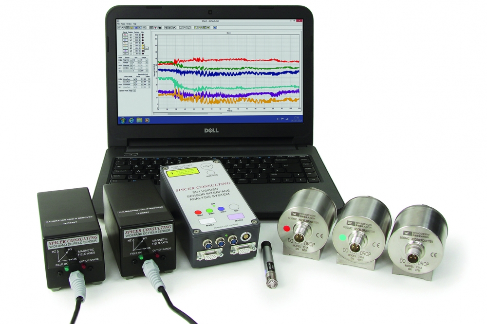
Accurate positioning of the scanning electron beam has a great impact on image quality; in practical applications, deviations of the beam cannot be larger than the examined part. Disturbances such as vibrations, or the electromagnetic interferences created by AC and DC sources, will all shift the position of the electron beam and decrease the resolution; AC fields show up as jagged lines in the image, while DC fields create wavy features. Unfortunately, these types of perturbations are quite common in environments where the semiconductors are produced and tested since, in order to save space, sensitive imaging instruments often have to share quarters with large pieces of industrial equipment. It is therefore important to perform an environmental survey prior to the installation of the electron microscope to ensure high quality imaging. Spicer Consulting, a leader in magnetic field cancellation, offers the SC11 Analysis System that has been designed for this task, measuring vibrations, acoustic waves and magnetic fields in the X, Y and Z directions. The results of these measurements are visualised graphically, helping the user to find the optimal location for their instrument.
Figure 1: The most simple way to alleviate magnetic interference is diagrammed above.

Figure 2: This diagram illustrates cable placement for enhanced interference mitigation.
Cancelling magnetic fields
Even if a microscope is installed in the part of a lab that shows the lowest interference, there will still be some disturbances; DC magnetic fields are always present, including the Earth’s field, and many instruments create AC fields with a frequency of ~60 Hz.
There are several ways to remove these magnetic fields. One of them is mu-metal shielding with metal sheets made from a ferromagnetic nickel–iron alloy with very high permeability. However, this solution is extremely expensive and has several limitations, as the material’s permeability decreases with suboptimal handling. A more reliable solution is to install an active magnetic field cancellation system that can be used to handle stray magnetic fields from the surrounding instruments, as well as the changes in the Earth’s field due to large moving ferromagnetic objects like elevators or metal doors. A common choice is Spicer’s SC24 system, which consists of a magnetic field control unit, one or more magnetic field sensors and 3-axis cables that can cancel out the detected fields.
Cable positioning
In application, the cables are positioned to form closed loops around the electron microscope – keeping the magnetic field around its column static. Cables can be positioned in different ways to find the optimal balance of complexity, cost and performance. The simplest and cheapest solution is to draw the cables (X, Y and Z) in three loops, forming three planes that do not intersect the microscope (figure 1), where the X and Y planes are parallel, and the Z plane is orthogonal to the column length. The benefits of this solution are that there are no cables on the floor, and no significant alterations to the room are required. However, the dynamic range and the cancelled volume are smaller, since the cables are further from the column. This set-up can be used for SEMs that have small columns and do not need a large volume of cancelled space that surrounds the instrument.
If better performance is required, the X and Y cables should cross the room directly above the microscope column (figure 2), since drawing the loops closer will enhance the system’s cancelling ability. For large TEMs or new labs, where remodelling would not disturb the other instruments, the optimal solution is to use dual loop cables and bury parts of them below the floor (figure 3). This solution gives the best performance and is recommended for TEMs with a Gatan Imaging Filter (GIF), since the GIF is situated below the microscope column and requires cancelling at a lower height. For existing microscope installations in which burying cables is not an option, the bottom sections of the cables can be at floor level and covered with suitable cable protectors. However, this will compromise the X and Y cancelling performance at GIF height.

Figure 3: For large TEMs, new labs under construction, or labs in which
remodeling won’t disturb normal operations, this diagram illustrates an
optimized interference mitigation solution that involves dual loop
cables and burying some cable portions below floor level.
Choosing the right sensors
The SC24 can be used with either one or two sensors of the same type. Using two sensors together, positioned on either side of the column, creates a ‘virtual’ sensor that measures the field at the spot of interest, by taking an average of the two measurements. The SC24 is available with two sensor types: SC24/AC for the detection of AC fields, and SC24/AC+DC for, as the name suggests, both AC and DC fields. The SC24/AC can cancel out disturbances with a frequency of 2.5Hz to 5kHz, with a cancelling factor greater than 50 at 60Hz, while the SC24/DC+AC can successfully cancel from 5kHz down to DC, with a cancelling factor of 100 at 60Hz and larger than 400 at DC.
Summary
Smaller semiconductors offer many benefits that continue to revolutionize OEM product development; semiconductors indeed impact almost every aspect of modern life. But the ever-shrinking size of ICs raises new challenges for manufacture and quality control (QC) testing. In order to properly investigate these components for defects, large degrees of magnification and exceptionally high accuracy are required. Electron microscopes offer a practical solution, but since they are very sensitive to changes in magnetic fields, it is important to cancel out any localised disturbances to ensure good image quality. Spicer Consulting provides instruments that can be used both to detect and to cancel the external magnetic fields, offering effective solutions that suit any lab or budget.
The Spicer Consulting SC24 offers multiple sensor choices and a wide range of frequency interference cancellation options.


