AEM introduces new generation of Automated Burn-In Systems

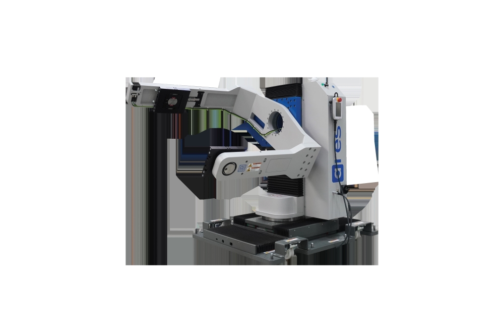
AEM has launched a new burn-in capability for its high-parallel test platform, AMPS.
The new variant, named AMPS-BI, is a high-power, high-throughput, fully automated burn-in system featuring patented advanced multi-zone Intelligent Thermal Control. AMPS-BI is designed to efficiently perform accelerated high voltage stress testing on advanced semiconductor devices such as AI processors and high-performance computing units.
High voltage stress testing is critical to ensure the reliability of AI chips and other semiconductor devices. It exposes devices under test to extended periods of operation under stressful conditions to detect potential failures or defects before reaching the end consumer. As AI processors and high-performance compute devices are manufactured with leading-edge process technology nodes and advanced heterogeneous packages with chiplets, the overall cost of test to provide the highest quality of the final package is increasing significantly. AMPS-BI leverages AEM's decades of experience in automation, thermal management, and application-specific test instruments to offer customers a scalable solution that reduces test times while increasing overall test coverage, delivering a cost-of-test advantage for its users.
AEM's AMPS-BI delivers:
• Fully automated modular system - Capable of simultaneous high voltage stress testing of hundreds of devices in parallel
• Patented Multi-zone Intelligent Thermal Control (ITC). Scalable to >2KW per device, with precision control for thermal stability during test
• Application-specific test instruments - Optimized for customer requirements to ensure optimal yield
• Individual device test control and instrumentation allow for asynchronous operation, pattern changing on the fly, and high system utilization
• Support for device-specific change kits and consumables, including burn-in boards and sockets
• Support for advanced package formats, scalable beyond 100mm x 100mm package sizes
• Upgradable for System Level Test, tri-temperature, and higher throughput
• Fully supports JEDEC-based I/O with full Factory 4.0 automation support
"As pioneers in the industry in providing cost-effective, highly parallel, modular automated test and handling solutions and with over a thousand systems installed worldwide for Burn-In and System Level Test, we are committed to delivering innovation and excellence to semiconductor testing," said Amy Leong, Chief Executive Officer of AEM. "I am incredibly proud of our team for developing this new generation of Burn-In (BI) systems, which will significantly help AI chip designers, foundries, and OSAT customers accelerate their roadmaps."
Earlier this year, AEM announced that its burn-in test system has been selected as the Plan-of-Record solution by a major fabless provider of high-performance compute (HPC) and artificial intelligence (AI) semiconductor chips.
AEM's Test 2.0 paradigm is at the forefront of test solutions for next-generation advanced logic devices, including high-performance compute and AI. AEM leads the industry in Active Thermal Control, Advanced Factory Automation, and Test Instrumentation.


