
KLA Launches New Double-Sided Direct Imaging Platform
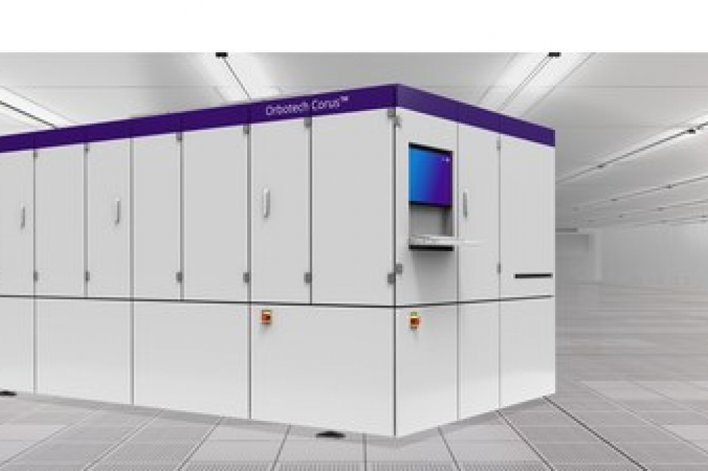
KLA Corporation has introduced the new Orbotech Corus 8M direct imaging (DI) solution, the first system built on the all-in-one revolutionary Orbotech Corus platform, combining the functionality and automation of an entire direct imaging production line in a closed, clean and compact unit. Providing increased resolution with high accuracy to pattern finer lines, the extendable Orbotech Corus™ DI platform is unique in its ability to support highly efficient double-sided imaging in a fully automated solution optimized for high throughput and capacity.
"PCB and IC substrate manufacturers are helping electronic device OEMs package increased functionality into their premium products while supporting a variety of form factors, and this requires increasing the density of transmission lines for advanced high-density interconnect PCBs and IC substrates," said Arik Gordon, general manager of the LIS division at KLA. "The all new Orbotech Corus DI platform provides this precise line forming capability at manufacturing throughput speeds and has achieved proven success in customer deployments. KLA's continued investments in precision DI technology will extend to future Orbotech Corus Series offerings as well, with additional enhancements planned for higher accuracy and resolution in upcoming years to continue enabling the IC substrate technology roadmap."
Orbotech Corus 8M DI systems enhance the field-proven Large Scan Optics (LSO™) and MultiWave™ Laser technologies with higher laser power, advanced optics and innovative scaling algorithms. This enables the Orbotech Corus 8M system to achieve fine resolution – down to 8µm line width – and higher registration accuracy of ±5µm for advanced applications. In addition, high depth-of-focus (DOF) ensures improved line precision and uniformity on varying surface topographies. The ability to produce ultra-fine lines with extreme accuracy makes the Orbotech Corus 8M ideally suited for the production of IC substrates (ICS) and advanced high-density interconnects (HDIs) for high-performance applications like premium smartphones and advanced wearable devices.
The Double-Sided Imaging (DSI™) technology provided with the Orbotech Corus 8M DI system facilitates the imaging of both sides of the PCB panel, eliminating the need for multiple independent DI, loader/unloader and flipper systems. With no external mechanical automation required, the fully integrated Orbotech Corus 8M DI system enables higher throughput capacity per square meter than traditional DI lines, and greater process uniformity.
This innovative solution is equipped with advanced target acquisition capabilities including the ability to recognize and process a high number of targets with any target layout across the panel with minimal throughput loss.
In addition, the fully integrated system reduces contamination risk by including integrated cleaners and filters all in an enclosed 'box', helping to provide a clean environment throughout the system and even higher cleanliness in the exposure area of the tool to maintain high yield levels.


