+44 (0)24 7671 8970
More publications     •     Advertise with us     •     Contact us
 
Loading...
News Article

Advantest Unveils E5620 DR-SEM for Review and Classification of Ultra-Small Photomask Defects

News

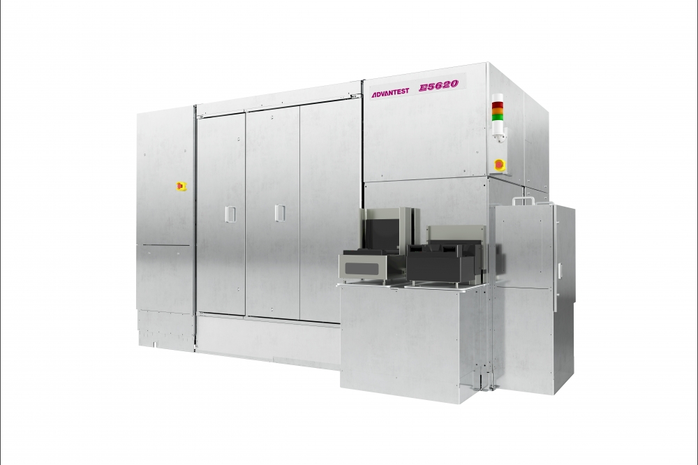
Semiconductor test equipment supplier Advantest Corporation unveiled the E5620 Defect Review Scanning Electron Microscope (DR-SEM), its newest mask SEM product for reviewing and classifying ultra-small defects on photomasks and mask blanks. With its high-accuracy, high-throughput defect review capability, the E5620 DR-SEM is expected to contribute appreciably to production quality improvements in next-generation photomasks and shorter mask manufacturing turnaround times.

Like its predecessor, the E5620 implements Advantest’s highly stable image capture technology to easily import defect location data from mask inspection systems and automatically image the locations. The system has a number of improvements specifically to target future mask requirements.

“In working with our customers to determine their requirements for the future EUV photomask inspection and analysis, we identified several essential advancements to integrate into our proven DR-SEM system,” said Toshimichi Iwai, senior VP of the Nanotechnology Business Group with Advantest. “With the E5620, our team of lithography experts has created a superior tool that can handle today’s photomasks and is truly future-ready for the coming EUV generation.”

E5620 Key New Features

· High Spatial Resolution

· Highly Stable, Fully Automatic Image Capture

· Compatible with Mask Inspection Systems

· Elemental Composition Analysis Option

· Backscattered Electron Analysis Option

The E5620 DR-SEM is available for purchase now. Advantest will share further details regarding its new E5620 DR-SEM during SEMICON Japan 2022, December 14-16, at Tokyo Big Sight. To learn more, please visit the company in booth 1549 during the show.

SPEA donates test equipment to university in Thailand
SONOTEC and S3 Alliance join at SEMICON Europa
Luminaries like high-NA EUV and curvilinear photomasks
SensiML and Silicon Technology join forces
TRI launches high-performance 3D AXI
SONOTEC and S3 Alliance join at SEMICON Europa
Marquee Semiconductor expands Indian presence
Micron begins Memory Manufacturing Fab
SiLC Technologies advances Machine Vision
Renesas partners with EdgeCortix
Gradiant acquires H+E Group
Webinar: Hydrogen Generation Industry Innovations to Meet Expanding North American Fab Hydrogen Requirements
EdgeCortix set to disrupt the edge market?
Evonetix places first DNA Synthesis Development Platform at Imperial College London
ASE launches Integrated Design Ecosystem
Cohu acquires Equiptest Engineering
Advantest wins 2022 Best Supplier Award from ASE Holdings
SEMI welcomes new board members
Advanced Energy breaks ground on flagship factory
GlobalFoundries opens new Malaysia office
TSMC reveals 'breakthrough' set to redefine the future of 3D IC
Delphon announce new VP, strategic marketing & business development
Particle Measuring Systems Announces Acquisition of EMS
Ireland begins high-volume production of Intel 4 Technology
Advantest to showcase latest test solutions
200 gigabits per second
KemLab Inc. applauds CHIPS Act's commitment
200mm fabs to reach record capacity by 2026
Governor DeSantis dedicates $50 million for workforce development
DOD names eight 'Microelectronics Commons' Hubs
TSMC accelerates renewable energy adoption
Mouser signs global agreement with MediaTek
×
Search the news archive

To close this popup you can press escape or click the close icon.
Logo
×
Logo
×
Register - Step 1

You may choose to subscribe to the Silicon Semiconductor Magazine, the Silicon Semiconductor Newsletter, or both. You may also request additional information if required, before submitting your application.


Please subscribe me to:


You chose the industry type of "Other"

Please enter the industry that you work in: