Trends in the semiconductor industry
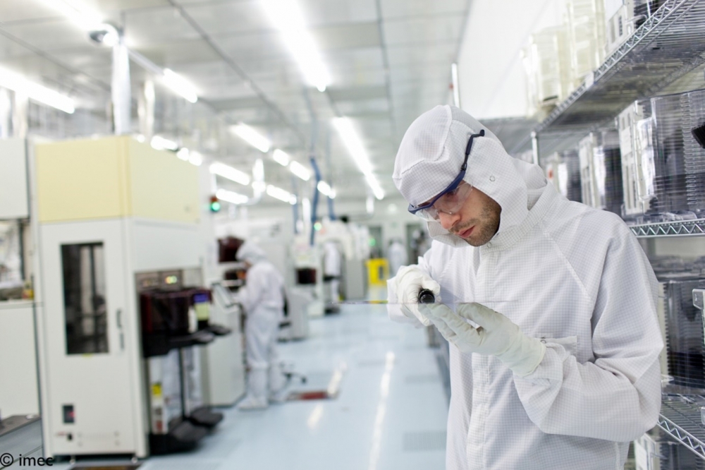
Sri Samavedam, senior vice president of CMOS technologies at imec, reviews important semiconductor industry trends
Which are the new innovations in logic CMOS scaling that will be introduced in industry in the coming years?
Using the wafer backside for power delivery to the devices is the next major performance booster that will be introduced. The conventional metal layers on the frontside of the wafer will be used for routing signals, while the metal layers at the back of the wafer will be used for power delivery. Separating the power delivery and signal routing enables lower voltage drop in the power supply (which improves performance) and reduces congestion of metal routing on the frontside. Intel has announced that they will introduce this at the 2nm node with nanosheet devices.
TEM image showing scaled FinFETs connected to the wafer’s backside and frontside.
The device architecture beyond nanosheets and forksheets is complementary FETs (CFETs) where N and P devices are stacked on top of each other using a complex integration. There are several flavours of CFETs possible, and we are in the early stages of pathfinding. There are several flavours of CFETs possible, and we are in the early stages of pathfinding. In the back-end metallization, copper dual-damascene integration will give way to high aspect ratio metal etch to pattern lines below 20nm pitch. We have been focusing on enabling Ruthenium for direct metal etch. To lower the resistance, the aspect ratio of Ruthenium will be increased along with airgaps to reduce the capacitance impact. These changes will ensure that the back-end RC (resistance-capacitance) scaling roadmap continues for several nodes.
As scaling becomes more challenging what trends are you observing in the industry?
Scaling of logic and memory components is getting harder. The node-to-node improvement is diminishing even as costs continue to increase due to integration complexity. On the design side, there is a trend to create more domain specific accelerators for each function like neural processing, graphics, video, etc. and a much stronger focus on hardware-software co-optimization to gain more at the system level.
There is also a drive to identify specific technologies to address system bottlenecks like the memory wall (how to get data at high bandwidth, with sufficient speed and low enough power to feed the logic cores), power wall (how to efficiently handle power delivery and thermal dissipation) or datacom bottlenecks (how to ensure wired, photonics and wireless infrastructure can handle the exponentially increasing data traffic) instead of relying on off-the-shelf generic technologies.
There is a drive to identify specific technologies to address system bottlenecks like the memory wall, power wall or datacom bottlenecks instead of relying on off-the-shelf generic technologies.
There are examples in high-performance compute space like AMD’s V-cache technology where 3D integration is used to bring extra SRAM memory closer to the CPU. Another example is the use of a silicon interposer bridge to connect two CPU die in the Apple M1 Ultra system-on-chip (SoC). There is also a strong push to co-package the electronic and photonic ICs leveraging different 3D and 2.5D technologies to reduce parasitic electrical resistance as data bandwidths increase in optical IO systems. When it comes to 3D and 2.5D connectivity, there are several options depending on the density of connections, cost, and complexity. The equipment, metrology and EDA infrastructure also needs to be mature to drive standardization and reduce cost for broader adoption.
How is imec planning to address the industry trends that you highlighted?
The imec design technology co-optimization (DTCO) program works on design benchmarking across logic, memory, and 3D to build technology influenced process design kits (PDKs) for future nodes. In the system technology co-optimization (STCO) program we use these research PDKs to address system challenges like the memory wall and the power wall. For example, we work on the 3D partitioning of domain specific SoCs and perform multi-scale thermal analysis including different cooling solutions and hybrid memory implementations.
To address the maturity of 3D technologies we are partnering closely with key equipment suppliers and working with Cadence to enable electronic design automation (EDA) tools needed for true 3D partitioning of SoCs.
Can you give some examples of promising CMOS R&D topics that imec is focusing on?
In logic, we continue to explore and benchmark various integration and module options for realizing CFET devices, which are expected to enable 4T standard cell designs. In the backend, there is progress in incorporating airgaps in high aspect-ratio metal lines to enable RC scaling. In the realm of quantum computing, we work towards lowering charge noise in silicon spin qubit devices which is very promising for high fidelity qubit operation for quantum computing.
In the backend, there is progress in incorporating airgaps in high aspect-ratio metal lines to enable RC scaling.
As the data rates supported by optical IOs increase, the electric IC and the photonic IC are more closely integrated using co-packaged optics to reduce parasitics. We are developing new modules to making co-packaged optics a reality.
In the active memory program, we continue to improve the device performance and reliability of IGZO (indium-gallium-zinc-oxide) devices, which will play a key role in future scaled DRAM architectures. In our storage program, we keep on pushing the conventional gate-all-around 3D NAND Flash scaling roadmap for storage applications.
How is imec contributing to a more sustainable society?
Imec takes a broad and holistic approach towards sustainability. In our operations we plan to reduce our carbon footprint by 65% by 2030 and we are progressing well towards this goal. In addition, we promote a healthy work-life balance with a strong safety culture, and we use the UN sustainable development goals as a compass for research projects. We do research in production of renewable energy like green hydrogen and photovoltaics.
Last year we launched our sustainable semiconductor technology and systems (SSTS) program aimed at quantifying and mitigating the carbon footprint of semiconductor manufacturing across logic, memory, and 3D integration flows.
Our sustainable semiconductor technology and systems (SSTS) program aims at quantifying and mitigating the carbon footprint of semiconductor manufacturing.
Our goal is to bring together the entire semiconductor ecosystem to address this global challenge. So far, several leading partners such as Apple, Amazon, Microsoft, ASM, ASML, Kurita, Screen, Tokyo Electron have joined this program. We hope to announce several other equipment, foundry, and system partners soon. We are partnering with the SEMI Sustainability Advisory Council to share the learnings and best practices broadly to encourage adoption among industry leaders.
About Sri Samavedam
Sri Samavedam is senior vice president of CMOS technologies at imec since August 2019. His responsibilities include programs in logic, memory, photonics and 3D integration. Prior to that, he was senior director of technology development at GlobalFoundries in Malta, NY, where he led qualification of 14nm FinFET technology and derivatives into volume production and early development of 7nm CMOS. He began his research career at Motorola in Austin, TX, working on strained silicon, metal gates, high k dielectrics and fully-depleted SOI devices. He holds a Ph.D. in Materials Science and Engineering from MIT and a masters from Purdue University.


