Fraunhofer IPMS presents latest photonic technologies
Digitalization, automation and efficiency are the buzzwords of the industry of the future. To this end, the Fraunhofer Institute for Photonic Microsystems IPMS develops customer-specific sensors, actuators and optical components. These represent the key technologies for IoT and numerous future applications with artificial intelligence.
Fraunhofer IPMS is one of the leading research institutes for the development and manufacture of electronic, mechanical and optical components and devices and their integration into intelligent systems. With its innovative micro-electro-mechanical systems (MEMS) and micro-opto-electro-mechanical systems (MOEMS), the institute opens up new applications through improved properties and additional functions, such as smaller dimensions, greater energy efficiency and higher performance.
Photonic microsystems for optical light control
The photonic systems of Fraunhofer IPMS can modulate light by means of small deflectable mirrors and thus generate images and structures in a unique way. For this purpose, the research institute develops spatial light modulators with up to several million mirrors on a semiconductor chip. The main areas of application for those mirror matrices are in the fields of microlithography in the deep ultraviolet range, production of printed circuit boards (PCB), semiconductor inspection and measurement technology, as well as in adaptive optics, astronomy, holography and microscopy. With its developments in this field, Fraunhofer IPMS is currently a world leader.
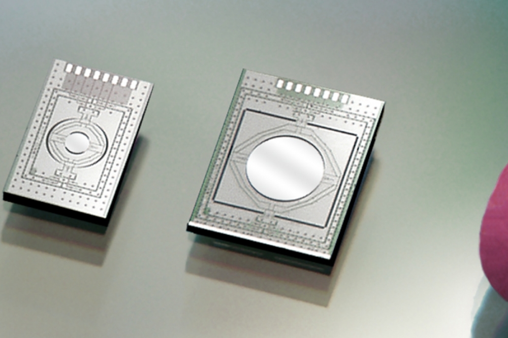
Customized, highly miniaturized MEMS scanners
Fraunhofer IPMS has many years of experience in the development and manufacture of customized, highly miniaturized MEMS scanners. The devices feature large scan angles and high scan frequencies and show excellent long-term stability. Applications can be found in scanning imaging, laser scanning microscopy, endoscopy, LiDAR sensor technology for autonomous driving or in head-up displays, head-mounted displays as well as AMR displays.
One of the institute's latest developments are the first hybrid 2D vector scanner modules with electromagnetic drive. They allow 2-dimensional quasi-static deflection at larger mirror apertures as well as high vectorial positioning speed. "This new approach significantly expands the parameter space of previous monolithic scanners. At the same time, the established advantages of Fraunhofer IPMS scanner mirror technology - high optical planarity and decoupling of the scan axes through gimbal suspension as well as the fatigue-free nature of the spring elements - are retained," explains Dr. Jan Grahmann of Fraunhofer IPMS.
Based on the scanner technology, a spectrometer has been developed that reliably detects solid, liquid and gaseous substances in real time. The current system addresses the proven spectral range from 950 nm to 1900 nm with a spectral resolution of 10 nm. Currently the system reaches a construction volume of about 2 cm³. However, further miniaturization is possible. A demonstration system shows the detection of white powders. This could be salt, sugar, starch or flour. However, numerous other substances that appear visually similar can also be reliably detected and assigned. Applications range from the detection of pharmaceutical and chemical substances to hazardous materials and recycling.
The Fraunhofer IPMS microscanners are also the centerpiece of a novel laser scanning microscope for tumor delineation. With its help, cancer operations can be made faster, more precise and safer. While still in the operating room, the doctor can use the microscope to examine the tissue from which the tumor has just been excised. A fluorescent marker applied beforehand makes visible any cancer cells that may have remained after the incision. These can then be removed completely and precisely. The surrounding tissue is spared, because the microscope display shows exactly where the healthy tissue begins. And no one has to wait for a laboratory result.
Fraunhofer IPMS will be presenting this research from January 31 to February 2 at the world's leading photonic technology trade show - SPIE Photonics West - in San Francisco. There, at booth Hall E #3387, visitors will also receive information about the institute's developments on integrated optical biosensors for point-of-care applications in medicine and on a contact-free medical radar for patient monitoring.