+44 (0)24 7671 8970
More publications     •     Advertise with us     •     Contact us
 
Loading...
News Article

High precision and high resolution

News

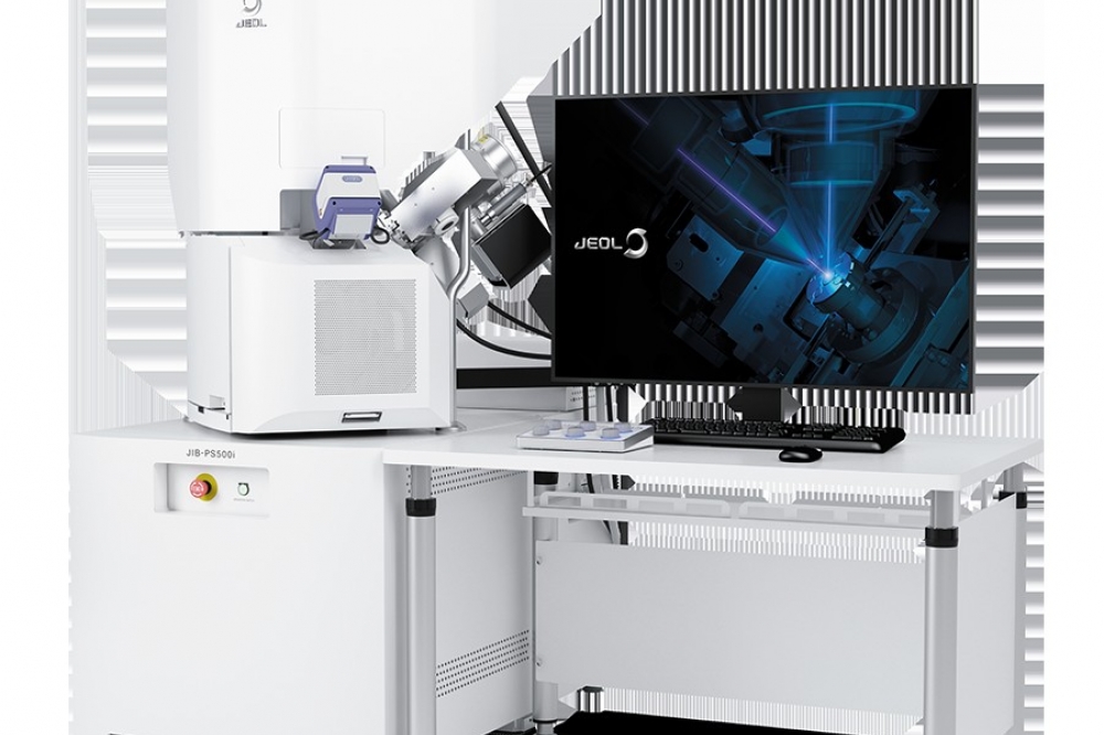
JEOL launches the FIB-SEM System “JIB-PS500i”.

With the finer structure of advanced materials and advancing complexity of processes, evaluation techniques such as morphological observation and elemental analysis require higher resolution and precision. In the preparation of samples for transmission electron microscopes (TEM) in the semiconductor industry as well as in the battery and materials fields, "higher precision" and "thinner sample" are required.

This product is a combined system of the FIB (Focused Ion Beam) system that can process with high accuracy and the SEM (scanning electron microscope) of high resolution to satisfy these needs.

Main Features

1. The FIB column enables processing with a large-current Ga ion beam up to 100nA. The high-current processing is particularly effective in preparing cross section samples for large-area imaging and analysis. In addition, the FIB column is set to a shorter working distance. Along with a newly-developed power supply, it has led to greatly improved processing performance at a low accelerating voltage.

2. A newly-developed super conical lens system is built into the SEM column, greatly improving the image resolution at a low accelerating voltage. This superb imaging is very useful to check the end-point milling status of lamella specimen using the SEM.

3. The JIB-PS500i adopts a large specimen chamber and a newly-developed specimen stage, increasing the stage movement range, and thus accommodating a large specimen.

In addition, a newly-developed STEM detector that can be used with the stage tilt at 90 degrees, allows for a seamless transition from the TEM specimen preparation to STEM observation.

4. For the operating GUI, the “SEM center”, which has been well received in the JSM-IT800 series of high-resolution scanning electron microscopes is employed, enabling full integration of EDS analysis.

5. A double tilt cartridge and a dedicated TEM holder allows for more precise alignment while making specimen transfer between TEM and FIB easier.

Reality AI Explorer Tier offers free AI/ML development access
AEM introduces new generation of Automated Burn-In Systems
NPUs are emerging as the main rival to Nvidia’s AI dominance, says DAI Magister
Camtek receives a $20M order from a Tier-1 OSAT
Free samples of every STMicroelectronics NPI IC available from Anglia
NY CREATES and SEMI sign MoU
Major government investment to 'propel' Canada
QuickLogic announces $5.26 million contract award
ASNA and Athinia collaborate
Global sales forecast to reach record $109 billion in 2024
AMD to acquire Silo AI
Nanotronics unveils 'groundbreaking' Gen V AI Model
Aitomatic unveils SemiKong
Biden-Harris Administration reveals first CHIPS for America R&D facilities and selection processes
Collaboration to produce cutting-edge AI accelerator chips
Oxford Ionics breaks global quantum performance records
Adeia wins ECTC Award for paper on “Fine Pitch Die-to-Wafer Hybrid Bonding”
AEM introduces new generation of Automated Burn-In Systems
Sydney council forges vital semiconductor agreement
EV Group's EVG880 LayerRelease wins 2024 Best of West
Biden-Harris Administration to invest up to $1.6 billion
Cyient sets up subsidiary for semiconductor business
EMD Electronics network leaders honoured
Accenture acquires Cientra
Introducing Park FX200
Deep learning chipset market to surge to $72.8 billion by 2033
PI Innovation Award 2024: Nanobodies for Diagnostic and Therapeutic Applications
Graphcore joins Softbank Group
Kaman Measuring highlights high precision displacement sensors
Si2 reveals recipients of Annual Power of Partnerships Award
Advantest achieves ASPICE Level 2 Certification for V93000 SmarTest 8 Software
Semiconductors to become a trillion-dollar industry by 2030
×
Search the news archive

To close this popup you can press escape or click the close icon.
Logo
×
  • 1st January 1970
  • 1st January 1970
  • 1st January 1970
  • 1st January 1970
  • 1st January 1970
  • 1st January 1970
  • 1st January 1970
  • 1st January 1970
  • View all news 22645 more articles
Logo
×
Register - Step 1

You may choose to subscribe to the Silicon Semiconductor Magazine, the Silicon Semiconductor Newsletter, or both. You may also request additional information if required, before submitting your application.


Please subscribe me to:


You chose the industry type of "Other"

Please enter the industry that you work in: