Enhancing deposition resistance
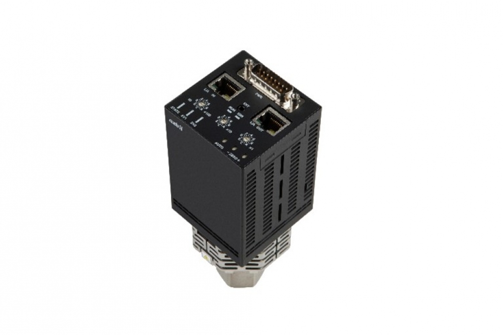
Azbil Corporation has introduced its model V8 sapphire capacitance diaphragm gauges, which employ MEMS processing technology to enhance resistance to deposition on the sensor.
As part of the continuing evolution of semiconductor manufacturing, the front-end film deposition and etching processes now use a wider variety of gases. Depending on the process gas used, film deposits may form on the sensor diaphragm of the vacuum gauge used in these processes, resulting in a shift of its zero point. Such a shift causes operators of film deposition and etching equipment to adjust the vacuum gauge more frequently, interfering with manufacturing plans.
Azbil has in the past developed products to deal with this problem, which continues to occur with the use of new gases. In seeking a better solution, Azbil has thoroughly redesigned its current sapphire capacitance diaphragm gauge and released the model V8, which has a sensor with a new structure, flow path, etc. MEMS technology is used to make the sensor chip’s surface uneven, helping to break up film deposited on the sensor diaphragm. Stress is now better balanced (also in models with an improved version of the flat sensor used in existing gauges), making the diaphragm surface less likely to flex. As a result, the amount of zero point shift in the model V8 due to film deposits has been dramatically reduced to one-tenth that of the existing model SPG.
The model V8S features a control unit that is separated from the gauge head, allowing use in temperatures as high as 250 °C. Such high-temperature environments are often found in atomic layer deposition (ALD) equipment due to changes in the process gas.


