
Texas Instruments selects Lehi, Utah
The historic $11 billion investment in manufacturing capacity further extends the company's cost advantage and provides greater control of supply.
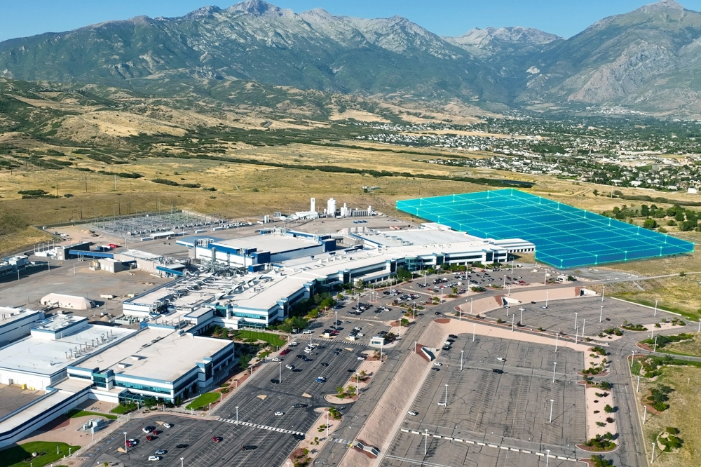
Texas Instruments Incorporated (TI) plans to build its next 300-millimeter semiconductor wafer fabrication plant (or fab) in Lehi, Utah. The new fab will be located next to the company’s existing 300-mm semiconductor wafer fab in Lehi, LFAB. Once completed, TI’s two Lehi fabs will operate as a single fab.
"This new fab is part of our long-term, 300-mm manufacturing roadmap to build the capacity our customers will need for decades to come," said Haviv Ilan, TI executive vice president and chief operating officer, and incoming president and chief executive officer. "Our decision to build a second fab in Lehi underscores our commitment to Utah and is a testament to the talented team there who will lay the groundwork for another important chapter in TI’s future. With the anticipated growth of semiconductors in electronics, particularly in industrial and automotive, and the passage of the CHIPS and Science Act, there is no better time to further invest in our internal manufacturing capacity."
The landmark $11 billion investment is said to mark the largest economic investment in Utah history. The Lehi expansion will create approximately 800 additional TI jobs as well as thousands of indirect jobs. TI looks forward to strengthening its partnership with the Alpine School District and will invest $9 million to improve student opportunities and outcomes.
"Companies like Texas Instruments continue to invest in Utah because of our world-class business climate and exceptional workforce," said Utah Gov. Spencer Cox. "TI’s new semiconductor fab will solidify Utah as a global semiconductor manufacturing hub for generations to come."
Lehi is an ideal location because of its access to skilled talent, robust existing infrastructure and strong network of community partners. The new fab will manufacture tens of millions of analog and embedded processing chips daily that will go into electronics everywhere.
The fab will be designed to meet one of the Leadership in Energy and Environmental Design (LEED) building rating system’s highest levels of structural efficiency and sustainability: LEED Gold. Plans include recycling water at nearly double the rate of the existing Lehi fab. Advanced 300-mm equipment and processes in Lehi will further reduce waste, water and energy consumption per chip.
Construction of the new fab is expected to begin in the second half of 2023, with production as early as 2026. The cost of the new fab is comprehended in TI’s previously announced capital spending plan to expand manufacturing capacity and will complement TI’s existing 300-mm fabs, which include DMOS6 (Dallas), RFAB1 and RFAB2 (both in Richardson, Texas), and LFAB (Lehi, Utah). TI is also building four new 300-mm wafer fabs in Sherman, Texas.


