
Stochastics metrology for HVM Fabs
FAME 300 series provides real-time monitoring of stochastic defects, helping HVM fabs to identify potential process problems within minutes.
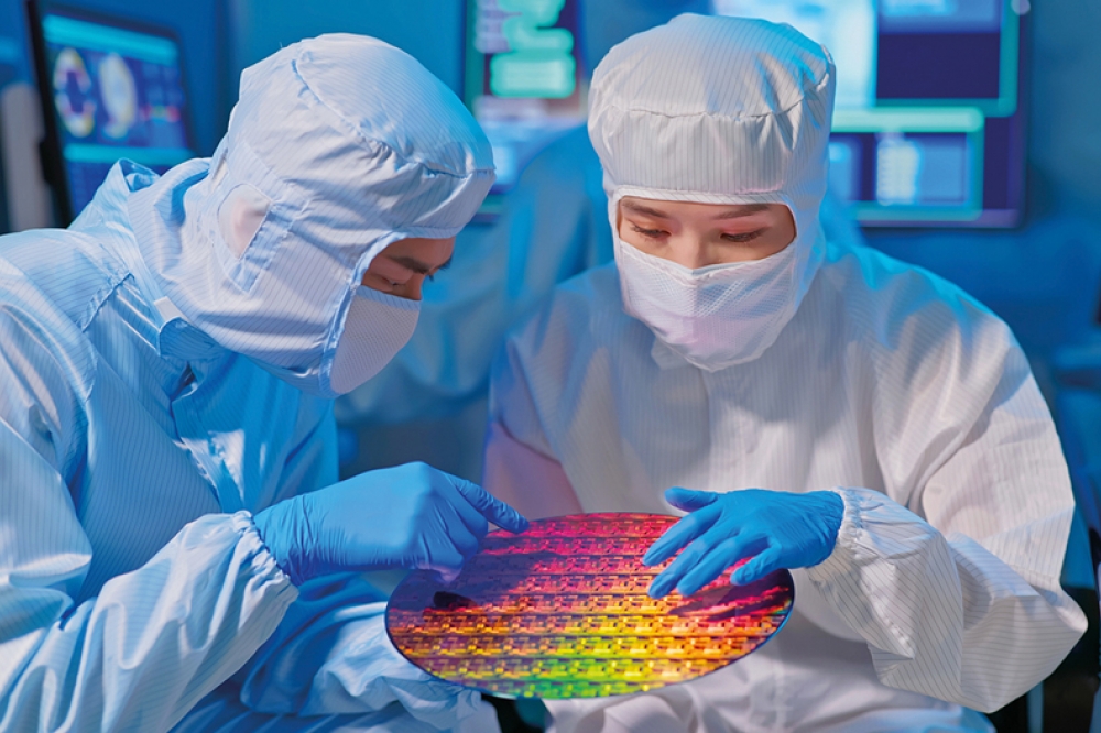
Fractilia has introduced the latest addition to its Fractilia Automated Measurement Environment (FAME™) portfolio, the FAME 300. Designed specifically for use in high-volume manufacturing (HVM) fab environments, the FAME 300 provides real-time measurement, detection and monitoring of stochastic effects, which are the single largest source of patterning errors at advanced nodes. With FAME 300, fabs can identify potential process problems caused by stochastic variations within minutes, enabling rapid corrective action to improve control over their patterning processes and optimize their yields.
FAME 300 utilizes Fractilia’s patented FILM™ technology, said to be the only fab solution that provides highly accurate and precise measurements of a wide range of stochastic effects as well as CD measurements. Fractilia’s products have been proven in R&D and process development environments among semiconductor manufacturers, equipment companies and materials suppliers. All measurements taken with Fractilia’s products can be transferred from R&D to HVM and can be fully automated.
“Leading-edge fabs are experiencing a significant rise in stochastic variations that will only get worse as the semiconductor industry tries to keep Moore’s Law moving forward with continued scaling. Stochastics must be measured accurately in order to be controlled so that new fab processes can be high yielding,” stated Fractilia CTO Chris Mack. “By integrating our FILM metrology engine into our new FAME 300 platform engineered for high throughput and reliability, as well as low latency, we can now bring our stochastics measurement capability to the fab HVM environment to enable our customers to better control their HVM processes, potentially saving months of product at risk from stochastics.”
The new FAME 300 platform leverages a Kubernetes cluster-based architecture that is highly scalable to achieve the throughput needed to measure all SEM images from across the entire fab. The FAME 300’s reduced latency enables fabs to obtain actionable data within minutes that can be used for feed-forward or feedback process control. Applications for FAME 300 include in-line mission critical use cases and HVM monitor use cases, and include lot dispositioning, real-time excursion detection, edge placement error optimization, lithography and etch process tool monitoring, SEM tool monitoring, SEM fleet matching, etch tool chamber matching, and many others. Fractilia has additional tool configurations for HVM monitor-only applications.
“Unbiased” Measurements Provide a More Complete Picture on the Wafer
Fractilia’s FAME portfolio of solutions uses a proprietary and unique physics-based SEM modeling and data analysis approach that measures and subtracts the random and systematic errors from SEM images to provide measurements of what is on the wafer rather than what is on the images. FAME measures all major stochastic effects simultaneously, including line-edge roughness (LER) / linewidth roughness (LWR), local CD uniformity (LCDU), local edge placement error (LEPE), stochastic defects, as well as many more. It provides the highest signal-to-noise edge detection in the industry (up to 5x higher signal-to-noise ratio than other solutions), and extracts more than 30x more data from each SEM image.
In addition, FAME works with all SEM tool vendors and all SEM tool models, and enables a 5-20x improvement in SEM tool-to-tool matching while simultaneously increasing SEM throughput by more than 30 percent. This unprecedented matching performance can be achieved not only across SEM tools of the same generation and type, but also between tools of different generations and even different tool vendors.
“Fractilia’s FILM technology is the industry standard for stochastics metrology,” stated Edward Charrier, CEO and president of Fractilia. “To date, we have more than 1,000 users of our FILM products in R&D at leading semiconductor device makers, major equipment manufacturers, materials suppliers, research consortia and others, with numerous proven use cases across optical proximity correction (OPC), lithography, etch, deposition, metrology and inspection, materials and other processes. Every year, the number of SEM images measured by customers using our products more than doubles. There is a clear need in the semiconductor industry to apply the accurate stochastics metrology that Fractilia has developed to HVM. That’s now possible with our new FAME 300 system, which enables our customers to control their HVM patterning processes more accurately and more robustly.”


