
Supporting data-intensive workloads
Ayar Labs shipping in-package optical I/O solutions with sub-10 nanoseconds (ns) latency and sub-10 Watts of power needed for leading semiconductor, AI/HPC and aerospace customers to support next-generation data-intensive workloads.
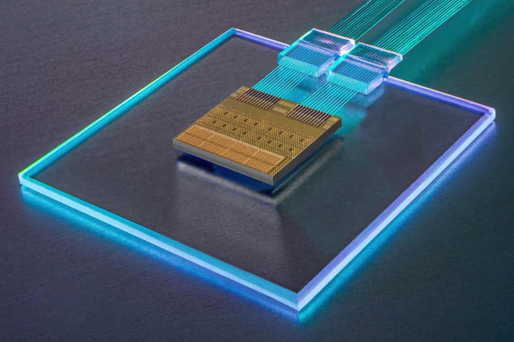
Ayar Labs has announced public demonstration of the industry’s first 4 terabit-per-second (Tbps) bidirectional Wavelength Division Multiplexing (WDM) optical solution at the Optical Fiber Communication Conference (OFC) in San Diego on March 5-9, 2023. The company achieves this latest milestone as it works with leading high-volume manufacturing and supply partners including GlobalFoundries, Lumentum, Macom, Sivers Photonics and others to deliver the optical interconnects needed for data-intensive applications. Separately, the company was featured in an announcement with partner Quantifi Photonics on a CW-WDM-compliant test platform for its SuperNova™ light source, also at OFC.
In-package optical I/O uniquely changes the power and performance trajectories of system design by enabling compute, memory and network silicon to communicate with a fraction of the power and dramatically improved performance, latency and reach versus existing electrical I/O solutions. Delivered in a compact, co-packaged CMOS chiplet, optical I/O becomes foundational to next-generation AI, disaggregated data centers, dense 6G telecommunications systems, phased array sensory systems and more.
“In-package optical I/O solutions have the potential to transform how semiconductor, AI, HPC and aerospace customers process their next-generation, data-intensive workloads,” said Craig Thompson, vice president of Business Development for Networking at NVIDIA. “NVIDIA’s accelerated computing platform is enabled by advanced technologies such as WDM optical interconnects to equip tomorrow’s innovators with the extreme performance they need.”
At OFC, Ayar Labs will have a first public demonstration showing its optical I/O solution moving data from one TeraPHY™ optical I/O chiplet to another at 2.048 Tbps each direction powered by their SuperNova light source. SuperNova powers 8 fiber links (using 64 highly accurate wavelengths operating at 32 Gbps, for 8 wavelengths and 256 Gbps per individual fiber) running error free at lower than 10ns of latency and without needing Forward Error Correction (FEC). This allows for a total bandwidth of 2.048 Tbps each direction, or 4.096 Tbps bidirectional. More importantly, the data transfer is using less than 5 pJ/bit (10W), a high level of energy efficiency, providing the power density and performance per watt needed to achieve AI models with trillions of parameters, advanced HPC designs and more.
“Ayar Labs continues to showcase our technology leadership with this live silicon demonstration, an industry-first milestone on the path to overcoming the impending power and performance wall of electrical design, and unleashing the power of next generation compute,” said Charlie Wuischpard, CEO, Ayar Labs. “As we bring together all the supply, manufacturing, test and compute pieces needed for high-volume deployment, we also show today that we continue to lead in pure technical achievement.”
“Revenue generated by Optical I/O for high performance computing (HPC) was around US$5 million in 2022 and is expected to reach US$2.3 billion in 2033 with a 74% Compound Annual Growth Rate for 2022-2033,”(1) explains Martin Vallo, Senior Analyst, Photonics, at Yole Intelligence, part of Yole Group. “Projections of rapidly growing training dataset sizes underline that data will become the main bottleneck for scaling machine learning (ML) models, resulting in a potential slowdown in Artificial Intelligence (AI) progress. Using optical I/O in ML hardware can help overcome this bottleneck, and could be the main driver for its adoption in next-gen HPC systems.”


