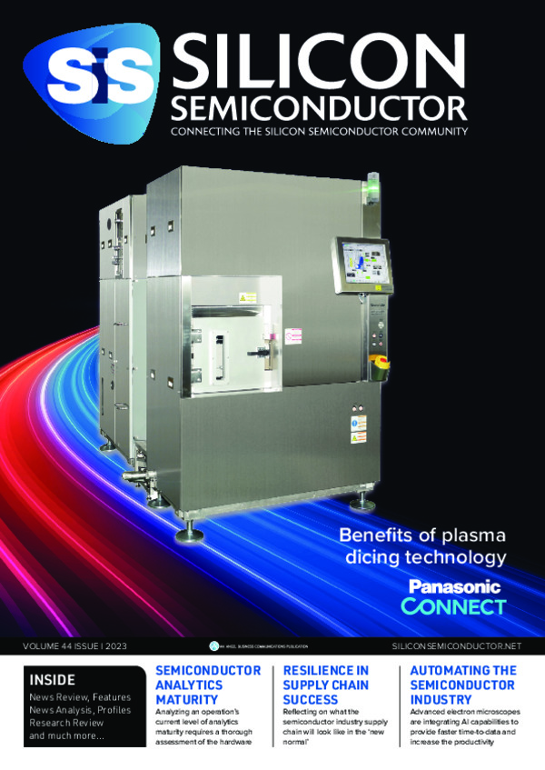
Benefits of plasma dicing technology
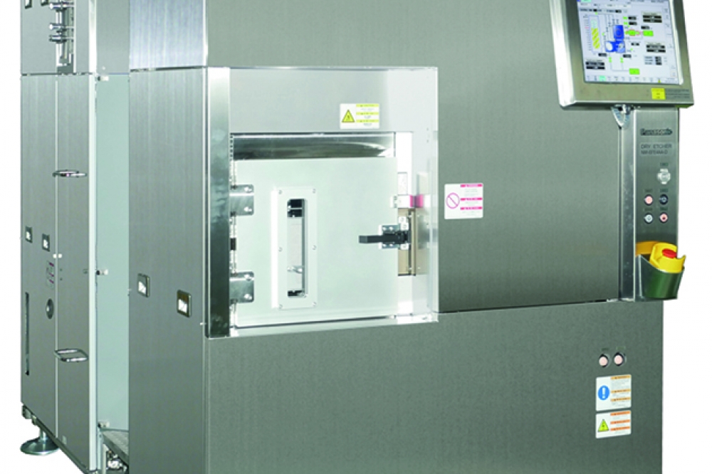
Plasma dicing addresses the challenges of dicing smaller and thinner dies; enables higher throughput and increased yield per wafer.
BY SHOGO OKITA, NORIYUKI MATSUBARA, ATSUSHI HARIKAI, and JAMES WEBER AT PANASONIC CONNECT
It could be argued that the defining feature of the Electronics Industry is the ability to miniaturize. Every person with a passing interest in electronics has heard of Moore’s Law: the processing power of affordable CPUs – or the number of transistors on a chip - will roughly double every two years. It is credit to both Gordon Moore’s foresight, and the technical and engineering teams around the world who continue to innovate, that the ‘Law’ is still even being discussed today. Part of the reason for chip size reduction lies in the shrinking of technology nodes (process geometries). Currently the smallest node that is being manufactured in mass volume is 7nm, and even the smaller size is under development in the industry.
The increase in processing power and speed and the miniaturisation and integration of electronic functions that continue to result from such technological advances lie at the heart of the pervasiveness of electronics in our everyday lives: the smart phones that we rely on; the uptake of artificial intelligence in smart homes and cities; driverless vehicles; remote medical home diagnostics – there is not one aspect of life that electronic products and systems have not penetrated.
But for this to continue, it is not only in the area of photolithographic processing that technology needs to keep innovating. Once a wafer has been created it must be singulated into individual dies, and as dies are becoming smaller and thinner, many products are facing difficulties caused by the singulation or dicing process. New challenges include: increasing material loss due to the width of the dicing street; mechanical damage such as chipping; and increasing processing time. Now, Panasonic has developed a plasma dicing process that in certain circumstances can replace mechanical dicing, which addresses these issues.
Types of Dicing Process
Traditionally, two dicing technologies have been used: scribing and breaking, and mechanical cutting using a dicing saw (“blade dicing”). Scribing and breaking causes stresses on the wafer and die and results in chipping and yield inefficiencies. Blade dicing also introduces stresses and contaminants which are more problematic as the die size and process geometries shrink. Laser dicing is another method which is faster than using a saw, but can also cause cracking and damage to the chip.
Now, a new dicing process has been introduced which uses a plasma chemical etching process, where all the ‘cuts’ are achieved in a single batch process, with no die stressing, no contamination, and an increase in wafer dicing throughput. Also, more chips can be designed onto the wafer as narrower dicing ‘streets’ can be used due to mask patterning. In addition, the mask pattern enables flexibility in the choice of chip sizes, shapes, positioning. The two approaches are shown in Figure 1.
Figure 1. Blade Dicing & Plasma Dicing Processing
Figure 2 shows Panasonic’s plasma dicing process which uses a dicing mask. The plasma process etches the streets by chemical reaction. Plasma dicing uses pulsed or time-multiplexed etching, with the process cycling repeatedly between two phases: a near-isotropic plasma etch where ions attack the wafer in a near-vertical direction; followed by the deposition of a chemically inert passivation layer which protects the entire substrate from further chemical attack. During etching, the vertically-directed ions attack the passivation layer only at the bottom of the trench (not along the walls), exposing the substrate to the chemical etch. This two-phase process results in side-walls that increase and decrease with an amplitude of between 100 and 500nm. The cycle time is adjustable: short cycles yield smooth walls; longer cycles yield a higher etch rate.
Figure 2. Panasonic’s chemical etch dicing process
Advantages of the plasma process over mechanical dicing
The action of the saw blade during the dicing process causes mechanical damage and affects inner layers of the die. Figure 3 demonstrates damage and chipping at the edge and of the inner layers. By contrast, the micro-photographs show no damage when the individual dies are separated using the plasma dicing process. Also, unlike blade dicing which causes micro particles of the wafer (e.g. silicon) to be freed up, potentially causing devices to fail, by using plasma etching, no contaminating particles are released.
Figure 3.Damage evident on chip samples using blade dicing (left); none present when plasma dicing is used
Greater chip strength
Chip breakage tests show the typical range of fracture strength for silicon chips to be in the range of 100MPa up to 3000MPa. Dies from several positions on a 150 µm thick wafer were sampled and a Weibull plot was used to compare the statistical data for chip strengths of lots using blade and plasma dicing preparation methods. Figure 4 shows that the plasma dicing process results in chips that are about five times stronger than those which underwent blade dicing. With a fracture stress pressure of 600MPa, all samples of chips that had been processed using blade dicing broke due to internal micro-cracks, whereas all of the plasma diced chips shattered at a pressure close to the breaking-strength of silicon.
Therefore the plasma dicing process is proven to result in dramatically higher chip strength, especially if thin wafers are being processed.
Figure 4. Strength tests prove the benefits of plasma dicing
Higher throughput and yield
The processing time of blade dicing depends on the number of dicing lines. If the die size is small, longer dicing processing time is required and throughput is reduced. However, with the plasma dicing process, etching is performed across the whole wafer in one pass, so throughput remains constant, no matter how many dicing streets are required (see Figure 5).
In addition, the plasma dicing process uses a narrower dicing street design. With blade dicing, there is always a minimum cutting street width, due to the thickness of the blade. A simulation prepared by Panasonic shows that for a 0.5mm² chip size, reducing the dicing street width from 60 µm to 5 µm, yield will be increased by 23% using the new plasma process. (See Figure 6). But how to avoid chips to contact others when handling wafer with 5 um dicing street width needs to be considered.
Figure 5. Productivity curves show increasing benefits with smaller chip areas
Suitability for different wafer processes
The Panasonic plasma dicing process can be applied to wafer dicing with mask patterning either performed by photolithography or laser patterning methods. The appropriate process flow should be selected to fit the wafer design (Figure 7).
Plasma dicing is a high quality innovation which offers different benefits depending on the end application, as shown in Figure 8. In small chips, for example, RF ID tags, IoT devices or MEMS sensors, the ability to obtain a higher number of chips per wafer, plus the reduction in process time is paramount. For devices such as image sensors, the elimination of contaminating particles is essential, and the smoother, damage-free sidewalls, with no heat-affected zones or cracking, allows an increase in the active area. For makers of memory ICs, the elimination of damage is most significant.
Figure 6. reduced street widths result in more chips/wafer
Panasonic Demo Centre
In order to demonstrate the plasma dicing process, Panasonic has built a customer demonstration centre in Osaka, Japan. This Class 1000 facility is capable of processing 200mm and 300mm diameter wafers with a minimum thickness of 25µm. It is fully-equipped including two APX300 plasma dicing machines, laser patterning equipment, polish grinder, lithography and measurement equipment, enabling customers to quickly and thoroughly evaluate different products and materials.
Figure 7. Panasonic plasma dicing process Applications
Conclusion
Panasonic’s plasma dicing process achieves damage-free and particle-free dicing, resulting in inherently stronger chips and increased yield. Throughput is increased and production costs reduced. Figure 9 summarises the different dicing processes and the advantages of the plasma dicing process.
Figure 8. Benefits of Plasma Dicing
All the data in this white paper have been verified in Panasonic’s Plasma Dicing Demo Centre in the company’s Smart Factory Solutions facility in Osaka, Japan, using the APX300 plasma dicer. Panasonic are continuing to develop the plasma dicing process for other materials such as silicon carbide, gallium arsenide and gallium nitride as well as silicon dioxide.
Figure 9. Summary comparison of dicing processes
Product Information
Panasonic can provide a plasma dicing total solution to achieve a damage-free, particle free, higher throughput and lower overall cost of production.
Panasonic Connect Europe GmbH
Caroline-Herschel-Strasse 100
85521 Ottobrunn, Germany
Tel. +49 89 45354-1000
microelectronics.sales@eu.panasonic.com
http://pfse.panasonic.eu


