Semiconductor Bonding Equipment market trends

The Semiconductor Bonding Equipment Market is expected to grow by registering a CAGR of about 6.1% during the forecast period.
Reportlinker.com has released the report "Semiconductor Bonding Equipment Market - Growth, Trends, COVID-19 Impact, and Forecasts (2023 - 2028)".
The increasing demand for semiconductor chips across various end-user verticals, along with the advancement in semiconductor packaging and assembling techniques, are driving the growth of this market.
Key Highlights
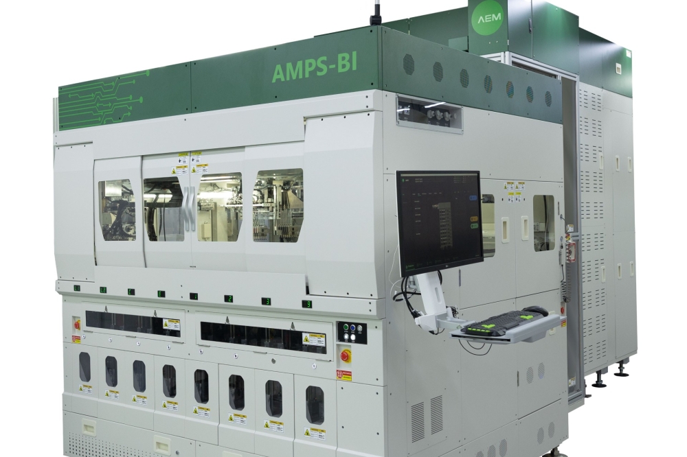
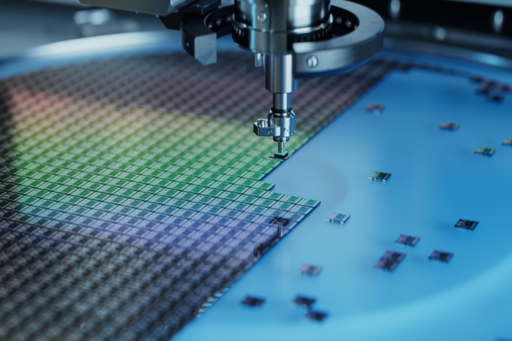
Semiconductor bonding is essential in chip manufacturing as it connects semiconductors and similar wafers to substrates/packaging materials. Wafer bonding has been critical in developing and successfully commercializing micromachined semiconductors, sensors, and actuators and is expected to continue to have an even more crucial role in developing and commercializing future ICs, microsystems, nanoelectronics, and other micromechanical systems.
Although, semiconductor bonding and inspection processes have historically been overlooked in favor of wafer fabrication due to obvious reasons such as high capital requirements and the criticality of the wafer fabrication processes. However, recent ad¬vancements in front-end equipment have significantly enhanced the importance of bonding and inspec¬tion equipment owing to the decreasing die size, lead counts, device speed, and finer pad pitches, making the performance of assembly and bonding equipment critical to all semiconductor companies looking to produce value-added products.
The increasing demand for semiconductor chips with higher efficiency, processing power, and smaller footprint has significantly changed semiconductor packaging and assembly techniques. For instance, methods such as stacked dye and 3D packaging are mainstream, driving innovations in the semiconductor bonding equipment market.
However, the studied market is facing some significant challenges as well; apart from the high cost of ownership of this equipment, the increasing complexity of the semiconductor manufacturing, packaging, and assembly processes also is challenging the growth of the studied market as the bonding equipment manufacturers need to design and develop equipment according to the requirement of the packaging/assembly types.
The outbreak of COVID-19 has had a considerable impact on the growth of the studied market, as the widespread lockdown imposed across various countries, especially in the Asia Pacific region, had a disruptive effect on the supply chain. Furthermore, the restrictions imposed on using a manual workforce further enhanced the intensity of the impact. However, with the results of the pandemic reducing to the lowest levels now, the semiconductor industry has been regaining momentum, which is expected to impact the studied market growth during the forecast period positively.
Semiconductor Bonding Equipment Market Trends
Advance Packaging to Hold a Significant Market Share
To meet new design and computing and design requirements demanded by emerging technologies such as 5G, IoT, AI, augmented and virtual reality, etc., it’s becoming crucial to enable high-density integration, reduced footprint, and enhance chip performance. Semiconductor manufacturers continuously focus on developing new processes and manufacturing techniques such as 3D through-silicon vias, heterogenous integration, and others to help meet these demands.
Such trends are thus driving the demand for advanced packaging and assembly equipment. For instance, according to SEMI, the sales in the assembly and packaging equipment segment were predicted to surge by 81.7% to USD 7 billion in 2021, followed by a further 4.4% increase in 2022, driven primarily by advanced packaging applications.
With advanced packaging continuing to gain steam, the semiconductor bonding equipment market is also expected to witness a similar growth trend, as semiconductor bonding is a crucial step for many technologies such as 3D integration, device stacking, wafer thinning (temporary wafer bonding), etc.
Asia Pacific to Hold a Significant Market Share
The semiconductor industry in the Asia Pacific region has witnessed remarkable growth in the last few decades. Countries like China, Taiwan, and South Korea have become the global manufacturing hubs for semiconductor chips.
Considering the presence of some of the largest semiconductor companies and the growing investment being made to support the semiconductor industry infrastructure across countries such as China, India, Vietnam, etc., the Asia Pacific region is expected to be among the major contributor to the growth of the studied market.
For instance, in December 2021, the government of India announced a PLI scheme of about INR 76,000 crores (~USD 10 billion) to support the growth of the semiconductor industry in the country. The program aims to provide attractive incentive support to companies engaged in Silicon Semiconductor Fabs, Compound Semiconductors / Silicon Photonics / Sensors (including MEMS) Fabs, Display Fabs, Semiconductor Packaging (ATMP / OSAT), and Semiconductor Design.
Such trends are expected to drive the demand for semiconductor equipment, including bonding equipment, in the region. According to SEMI, in 2022, China, Taiwan, and Korea are expected to remain the top three destinations for semiconductor equipment spending. While China is projected to maintain the top position next year, Taiwan is predicted to regain the lead in 2024. Equipment spending in most countries is predicted to witness a decline in 2023; the spending is expected to grow further as soon as 2024.
Semiconductor Bonding Equipment Industry Overview
The increasing demand for semiconductor bonding equipment drives competition in the studied market. The market has a mixed presence of established as well as new players. The new players are primarily betting on innovations to expand their clientele further, while the established players focus on increasing their market presence and portfolio further. Partnerships, especially in R&D, and mergers and acquisitions are among other significant strategies adopted by the vendors to strengthen their market presence.


