
Sample preparation time goes from hours to minutes
The microPREP PRO FEMTO system is said to enable micrometer-precision material removal at considerably higher speeds versus FIB milling while avoiding thermal damage to the sample.
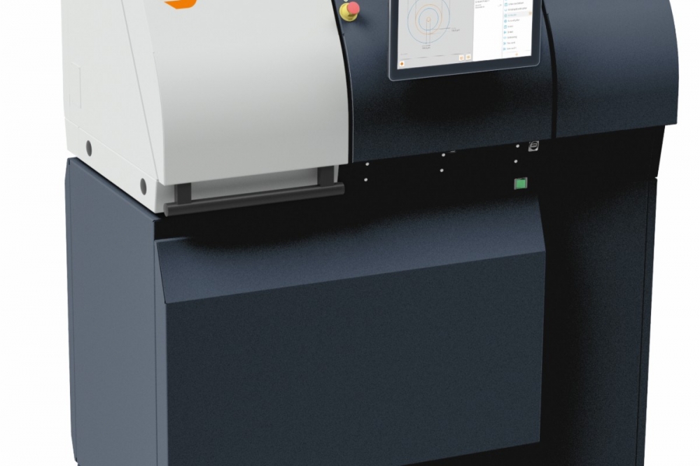
3D-Micromac AG has introduced the microPREP PRO FEMTO laser micromachining system for high-speed Atom Probe Tomography (APT) and cross-section sample preparation.
Fulfilling a critical need for atomic-scale materials analysis, the microPREP PRO FEMTO system features a femtosecond laser and optimized optical setup, which enables micrometer-precision removal of material in minutes versus many hours with focused ion beam (FIB) milling while avoiding mechanical and thermal damage to the sample. The microPREP PRO FEMTO enables APT microtip coupons to be prepared directly from the sample material with automated workflows. This frees up valuable FIB resources to be utilized more cost effectively for final preparation steps only, such as final annular focused milling and polishing of the microtips.
The Department of Materials Science at Montanuniversität Leoben (the University of Leoben), a leading research university in the fields of mining, metallurgy and materials science, has purchased the first microPREP PRO FEMTO system and is now using it for the preparation of APT specimens, focusing on a variety of different materials. According to Dr. Michael Tkadletz, Chair of Functional Materials and Material Systems at Montanuniversität Leoben, “APT is a crucial technique for the knowledge-based development of modern high-performance materials. For example, it can help to illuminate the segregation of impurities and tramp elements at grain boundaries of green steels, to reveal the complex elemental distribution within multifunctional coatings and nanostructures, or to investigate the effects of local chemistry on the performance of energy storage and conversion materials. Yet, the major bottleneck for APT experiments is the elaborate and time-consuming specimen preparation. Femtosecond laser preparation using the microPREP PRO FEMTO helps to overcome this bottleneck by reducing the complexity of the process, significantly reducing the time-to-sample and FIB utilization, while at the same time, the number of prepared specimens can be substantially increased compared to a standard lift-out-procedure.”
New Approaches Needed for APT Sample Prep
Traditionally, APT sample preparation processes have been based on electrolytic or ion-based thinning workflows. Both workflows require mechanical preparation steps that introduce mechanical stress to the specimen, which can affect the overall quality and yield. Using FIB milling for the preparation process to avoid mechanical stress can take many hours to complete and requires specialized lift-out of the specimen, which introduces risk of damaging the specimen. Since FIB systems are costly, this approach also ties up FIB resources and results in very high operational costs for the user.
Some systems combine a laser for high-speed ablation and an FIB for final polishing in a single platform. However, this approach creates capacity bottlenecks since only one process can be used at a time. In addition, since laser preparation ablates high volumes of material, particle contamination inside the analytic area of combination laser/FIB tools becomes a much bigger issue and its removal is difficult due to the vacuum conditions inside the isolated laser or process chamber. Short pulse lasers can also cause large heat-affected zones (HAZs), which can not only damage the sample but also can modify the structure of the probe tips, leading to inaccurate measurement results.
Unlike these other approaches, the microPREP PRO FEMTO is a dedicated laser micromachining solution that utilizes a femtosecond laser to provide the high speed, accuracy, cost-effectiveness, and versatility that research labs and universities require for APT sample preparation and cross-section analysis.
Dedicated Femtosecond Laser Micromachining
The microPREP PRO FEMTO can mill samples down to two microns from the final pillar – reducing APT sample preparation time from many hours to just minutes compared to FIB milling. Its femtosecond laser source limits the HAZ of the working sample to a few nanometers, compared to sub-micrometer-range HAZ with picosecond lasers. The system also features an optimized optical setup that includes a telecentric objective, which enables higher precision when preparing APT microtip coupons. This is especially important for coupons containing many APT pillars. The optical setup also features a shorter focal length and smaller laser spot size, adding to its high precision.
In addition, the microPREP PRO FEMTO features 3D-Micromac’s integrated proprietary CO2 Snow Jet contactless, non-abrasive cleaning system, which uses compressed air and dry ice in a normal atmosphere to safely remove particles from the surface of the sample following the laser preparation process. The microPREP PRO FEMTO also includes multiple pre-defined workflows, which facilitate setup and operation, and enable its use for a variety of use cases and applications.
“As materials science progresses deeper into the sub-nanometer and atomic scale, the demand for atom probe tomography for high-resolution and 3D-imaging-based materials analysis continues to grow. Prefabrication of microtip arrays for APT specimen preparation using a dedicated femtosecond laser ablation system can provide tremendous savings in time, effort and expense compared to mechanical sawing, FIB milling and short-pulse lasers,” stated Dr. Boris Arnold Rottwinkel, product manager microdiagnostics at 3D-Micromac. “By leveraging our expertise and technology leadership in laser micromachining solutions as well as in laser-based sample preparation through our microPREP PRO family, 3D-Micromac can offer research labs and universities a highly cost-effective, scalable and versatile approach to APT specific preparation to meet their growing and more demanding materials analysis needs.”


