
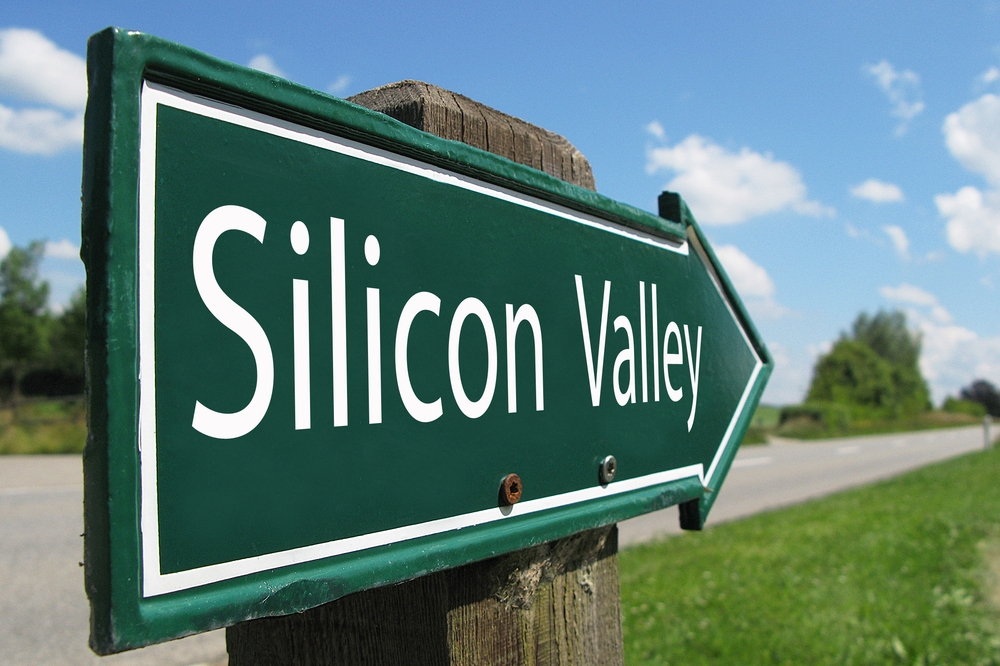
Noel Technologies ramps capacity at Silicon Valley fab
Semiconductor investments yield new tooling and cleanroom space at Campbell plant.
Noel Technologies, a Pure Wafer company, and a leading supplier of advanced semiconductor process development and fabrication services to the world’s top semiconductor integrated device manufacturers (IDMs), semiconductor original equipment manufacturers (OEMs) and fabless semiconductor companies, is undertaking a major expansion at its Campbell, California wafer fab. Pure Wafer is thought to be America’s number one supplier of silicon wafer reclaim solutions and services and the exclusive worldwide seller of films for Lam Research Corporation. Significant new investments in tools sets and clean room space at Noel Technologies’ Campbell fab are designed to meet increased demand from US semiconductor makers and their OEMs as well as support a sharp growth in demand for its MEMS and bioengineering development services.
Since 1996, Noel Technologies has served as an extension of semiconductor companies’ R&D organizations and their efforts to bring novel development and prototyping to market. Noel Technologies specializes in delivering process development optimization solutions for fabless semiconductor companies and OEMs. Its semiconductor engineering services serve as a production arm for advanced and highly sensitive process technologies, fostering a wave of innovation in the United States. This includes new semiconductor processing capabilities focused on semiconductor, bioengineering, MEMS, sensors, advanced packaging, and microfluidics products and devices.
“Customers have relied on the quality and know-how of our services and design methodologies for more than 26 years,” said S. Mark Borowicz, CEO of Pure Wafer. “We will continue to invest in advanced technologies to exceed those expectations and to always support the growth of our customers’ semiconductor and bio-engineering R&D groups. These groups have come to see us as an important bridge, serving as a valuable resource to complete key prototyping projects from development to full production.”
Expanded Cleanroom Adds Extensive Silicon Wafer Coverage from 50 mm to 300 mm
Noel Technologies supports the broadest range of wafer diameters, including 300mm, 200mm, 150mm, 100mm and 50mm tooling in its expanded cleanroom facility. As part of these investments in advanced technology, Noel Technologies increased its existing lithography capability by five times; processing 250um thick substrates to 2mm thick substrates, providing a wide range of multi-layer projects up to 10-12 layers and increasing its wet etch capabilities of silicon, dielectric and metal films. The expansion also adds a new range of plasma RIE Etch, dielectric and silicon process tools.
“Investments in process technologies and cleanroom capacity strengthens our unique lithography offerings, ramping up engineering support for reticle layout, and process development, which will ensure design success,” commented Brenda Hill, VP of Business Development. “These investments will further enhance our SEMI standards business, where we have become the industry leader of calibration standards for semiconductor equipment, in-situ processing of products for semiconductor manufacturing and process control.”


