+44 (0)24 7671 8970
More publications     •     Advertise with us     •     Contact us
 
Loading...
News Article

New foundry to accelerate quantum information research

News

The U.S Department of Energy's (DOE) Argonne National Laboratory has built the Argonne Quantum Foundry to accelerate advances in quantum information science.

The foundry is a national source of materials and data for quantum research that is unique in the Midwest.

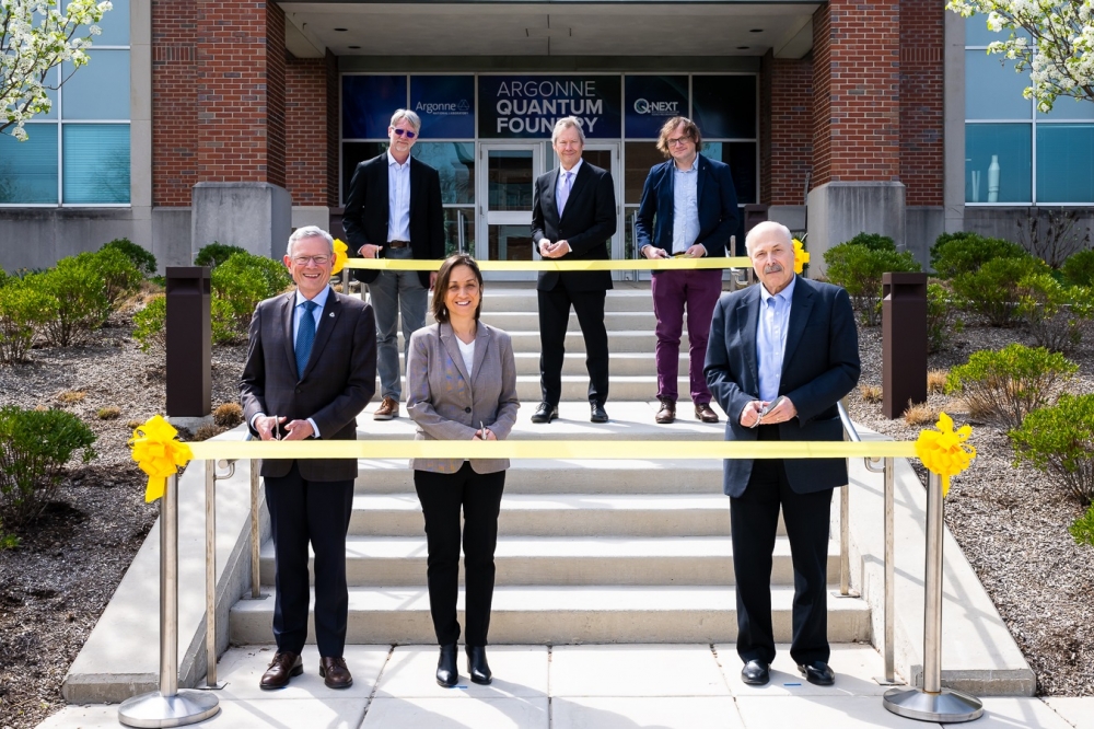
On April 19, Argonne marked its official opening at a ribbon-cutting celebration during which attendees toured the 6,000-square-foot research facility.

The creation of the Argonne Quantum Foundry was led by Q-NEXT, a DOE National Quantum Information Science Research Center hosted at Argonne. The foundry’s establishment and operation are a major part of Q-NEXT and set it apart as a quantum research center.

The foundry addresses the needs of the field on two fronts. One is to accelerate research.

In quantum information science, researchers turn nature’s quantum features, available only at atomic scales, to practical purpose. Quantum computers promise to solve today’s most intractable problems. Communication networks based on quantum technologies are expected to be unhackable.

At the foundation of these next-generation tools are sophisticated materials designed to store, process and distribute quantum information.

From a material’s creation to its incorporation into devices, the Argonne Quantum Foundry provides researchers with the tools to develop, test, fabricate and integrate novel forms of matter for quantum systems.

The second need is to strengthen the U.S. quantum ecosystem.

As a resource for the U.S., the foundry provides a robust, domestic supply chain of materials for both foundational science and industry research. Researchers within Q-NEXT, which include members of academia and industry, will be able to use the foundry. It will also be available for other national research efforts.

The Argonne Quantum Foundry focuses on a class of materials known as semiconductors. It features areas for developing, testing and fabricating semiconductor qubits, the fundamental components of quantum devices. It also features a prototype silicon-based quantum computer. The data collected at the foundry will be used to build a national database of materials and their properties.

Q-NEXT also led the establishment of a second foundry at DOE’s SLAC National Accelerator Laboratory. Its opening is imminent. It will focus on superconducting materials for quantum applications.

Tektronix and EA Elektro-Automatik offer expanded power portfolio
83% of supply chains can’t respond to disruptions in 24 hours
CMC Microsystems and ventureLAB sign MoU
Renesas introduces FemtoClock 3 timing solution
Mycronic receives order for SLX mask writer
Rapidus reveals US subsidiary and opens Silicon Valley office
Infineon introduces news MOTIX motor gate driver IC
Brewer Science unveils Smart Warehouse Monitor System
Symposium to showcase breakthroughs in microelectronics
CHIPS for America promotes over $50 million funding opportunity
SEMI University launches in-person courses
Samsung Electronics to establish Texan semiconductor ecosystem
Semiconductor chips drive innovation in AI and industries
Semiconductor equipment sales slip to $106.3 billion
Mouser Electronics receives 2023 Global Best Service Distributor of the Year Award from Diodes Incorporated
Quantum processor testing and measurement facilities up and running
Semiconductor Research Corporation announces 2024 call for research
Trend report unveils the future of circular electronics
PCIM Europe 2024: highlights and new records
PI contributes to technology node development
QP Technologies achieves ANSI/ESD S20.20 Certification
Renesas commences operations of Kofu Factory
TRI wins three Innovation Awards
Tektronix and recently acquired EA Elektro-Automatik offer expanded power portfolio
NEDO approves Rapidus’ FY2024 Plan and Budget
SK hynix signs Advanced Chip Packaging agreement
Renesas expands Quick Connect Studio
Infineon and Amkor deepen partnership
AP&S establishes site in the USA
Dracula Technologies selected by STMicroelectronics
RAIN RFID data to transform corporate sustainability initiatives
Integrated AMR replaces reed switches and hall effect sensors
×
Search the news archive

To close this popup you can press escape or click the close icon.
Logo
×
  • 1st January 1970
  • 1st January 1970
  • 1st January 1970
  • 1st January 1970
  • 1st January 1970
  • 1st January 1970
  • 1st January 1970
  • 1st January 1970
  • View all news 22645 more articles
Logo
×
Register - Step 1

You may choose to subscribe to the Silicon Semiconductor Magazine, the Silicon Semiconductor Newsletter, or both. You may also request additional information if required, before submitting your application.


Please subscribe me to:


You chose the industry type of "Other"

Please enter the industry that you work in: