
Alphawave Semi showcases 3nm connectivity solutions
Successful launch of 3nm connectivity silicon brings chiplet-enabled custom silicon platforms to the forefront.
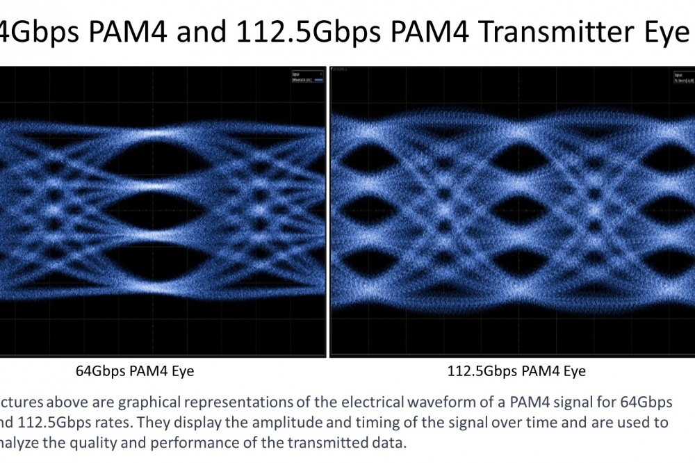
Alphawave Semi has announced the bring-up of its first connectivity silicon platform on TSMC’s most advanced 3nm process with its ZeusCORE Extra-Long-Reach (XLR) 1-112Gbps NRZ/PAM4 serialiser-deserialiser (“SerDes”) IP.
The 3nm process platform is crucial for the development of a new generation of advanced chips needed to cope with the exponential growth in AI-generated data, and enables higher performance, enhanced memory and I/O bandwidth, and reduced power consumption. ZeusCORE XLR Multi-Standard-Serdes (MSS) IP is the highest performance SerDes in the Alphawave Semi product portfolio and on the 3nm process will pave the way for the development of future high performance AI systems. It is a highly configurable IP that supports all leading edge NRZ and PAM4 data center standards from 1112 Gbps, supporting diverse protocols such as PCIe Gen1 to Gen6 and 1G/10G/25G/50G/100 Gbps Ethernet.
This flexible and customizable connectivity IP solution together with Alphawave Semi's chiplet-enabled custom silicon platform which includes IO, memory and compute chiplets, allows end-users to produce high performance silicon specifically tailored to their applications. Customers can benefit from Alphawave Semi’s application optimized IP-subsystems and advanced 2.5D/3D packaging expertise to integrate advanced interfaces such Compute Express Link (CXL™), Universal Chiplet Interconnect Express™ (UCIe™), High Bandwidth Memory (HBMx), and Low-Power Double Data Rate DRAM (LP/DDRx/) onto custom chips and chiplets.
“We are thrilled to be one of the first companies to successfully demonstrate our highest performance silicon platform with our XLR 112G Ethernet and PCIE6.0 SerDes IP on TSMC’s most advanced 3nm technology,” said Tony Pialis, CEO and co-founder of Alphawave Semi. “This represents a significant step forward in our execution of Alphawave Semi’s strategy to be a vertically integrated semiconductor leader in high-speed connectivity. Thanks to our rapidly growing partnership with TSMC through the Open Innovation Platform® (OIP), we continue to deliver innovative, high-performance custom silicon and IP solutions to our customers in data center, compute, networking, AI, 5G, autonomous vehicles, and storage applications.”
“Alphawave Semi continues to see growing demand from our hyperscaler customers for purpose-built silicon with very high-speed connectivity interfaces, fueled by an exponential increase in processing of AI-generated data,” said Mohit Gupta, SVP and GM, Custom Silicon and IP, Alphawave Semi. “We're engaging our leading customers on chiplet-enabled 3nm custom silicon platforms which include IO, memory, and compute chiplets. Our Virtual Channel Aggregator (VCA) partnership with TSMC has provided invaluable support, and we look forward to accelerating our customers' high-performance designs on TSMC's 3nm process.”


