
Fujifilm breaks ground on new €30 million European expansion
Expansion at FUJIFILM Electronic Materials (Europe) N.V. in Antwerp, Belgium, a manufacturer of materials used to make and modify patterns on silicon chips.
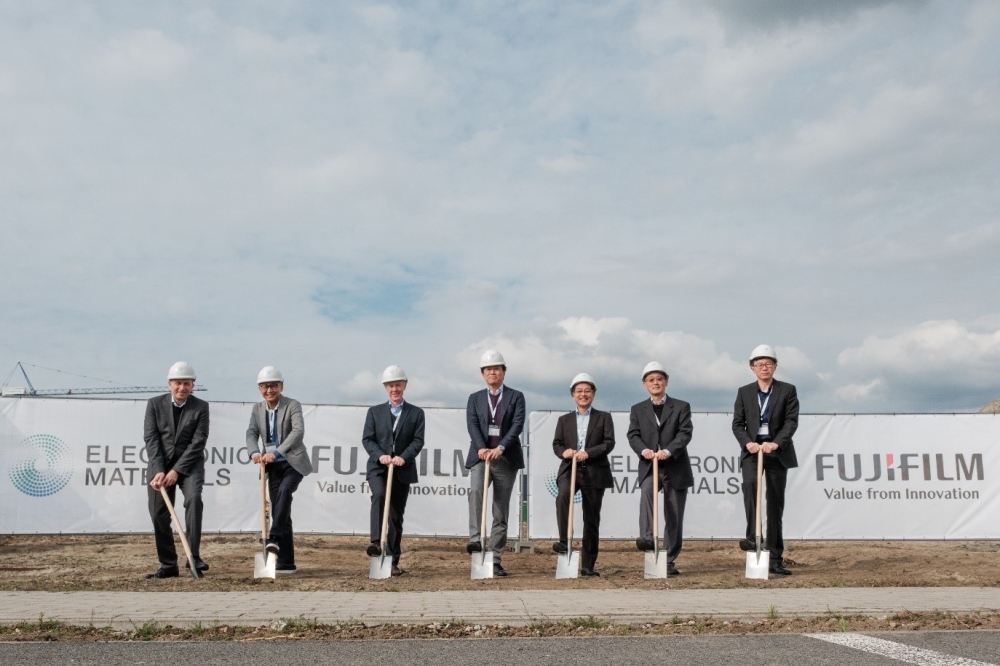
FUJIFILM Corporation (President and CEO, Representative Director: Teiichi Goto) has broken ground on a new €30 million expansion at its electronic materials manufacturing site in Belgium, FUJIFILM Electronic Materials (Europe) N.V., to grow semiconductor materials manufacturing capabilities in Europe. This marks one of Europe’s biggest capital expenditure investments in the semiconductor materials supply chain over the last decade.
This €30 million expansion will substantially increase the production capacity of FUJIFILM Electronic Materials (Europe) N.V., which manufactures core components and chemicals required for semiconductor manufacturing, including cleaners, polyimides, developers, and solvents. The 4000m² expansion project will also increase the space for clean room R&D and quality control labs by a third, while creating a new multi-purpose space for production and warehousing. Site enhancements will also see the addition of on-site solar panels, part of meeting environmental goals set out by Fujifilm’s Sustainable Value Plan 2030.
The expansion, targeted to be complete by the end of 2024, will create 25 new roles. Established in 1992 and acquired by Fujifilm in 2004, today, FUJIFILM Electronic Materials (Europe) N.V. employs more than 210 staff. New jobs created include production and lab roles, in addition to highly skilled technical and academic functions, and will appeal to a broad spectrum of candidates with STEM (Science, Technology, Engineering, and Mathematics) academic and professional backgrounds.
With the semiconductor market growing at an annual rate of 10%, Fujifilm has planned and announced the global investment of nearly €1 billion into its Electronic Materials business, including capital investment and R&D enhancements to meet expanding demand.
“This investment is an important milestone to accelerate further the growth of Fujifilm’s Electronic Materials business, which is the largest business in Fujifilm’s Advanced Materials segment,” said Tetsuya Iwasaki, General Manager, Electronic Materials, FUJIFILM Corporation. “As part of an overall investment package in Electronic Materials we have announced globally over the last several years, I am delighted that here in Europe, we are increasing our abilities to meet the growing short-and long-term needs of semiconductor manufacturers for world-class, innovative technology products.”
“As one of Europe’s biggest CapEx investments in the semiconductor material supply chain over the last decade, this expansion is an important part of developing the European semiconductor ecosystem, which will be crucial for society in delivering cutting-edge future technologies across the fields of automotives, energy management, healthcare, business, and current and future digital industries,” said Hans Vloeberghs, President & Managing Director, FUJIFILM Electronic Materials (Europe) N.V. “In addition to increasing our productivity, speed, and efficiency to produce leading-edge chemical formulations that power the most critical processes of semiconductor technology for our European customers, here in Belgium, I am proud that this investment will create 25 new exciting STEM jobs, enhancing our highly-skilled, high-value workforce.”
With the overall semiconductor industry projected to reach $1 trillion by 2030, Fujifilm will continue building upon its foundation as a semiconductor manufacturing supply chain leader, anticipating its significant growth.


