
Micron to bring EUV technology to Japan
1-gamma to be produced in Micron’s Hiroshima fab.
Micron Technology will be introducing extreme ultraviolet (EUV) technology to Japan, tapping this sophisticated patterning technology to manufacture its next generation of DRAM, the 1-gamma (1γ) node. Micron will be the first semiconductor company to bring EUV technology to Japan for production, with its Hiroshima fab playing a critical role in the company’s development of the 1-gamma node. Micron expects to invest up to 500 billion yen in 1-gamma process technology over the next few years, with close support from the Japanese government, to enable the next wave of end-to-end technology innovation such as rapidly emerging generative artificial intelligence (AI) applications.
With each successive advancement in process technology to scale memory cells and advance performance, Micron enables increased memory density, improvement in power efficiency and lower cost per bit, helping to unlock new opportunities for digitization, sustainability and green transformation, and automation. The introduction of 1-gamma follows the development of Micron’s 1-beta (1β), the industry's most advanced DRAM node today, which Micron mass produces in its Hiroshima fab. Micron continues to make progress on its EUV integration plans and expects to ramp EUV into production on the 1-gamma node in Taiwan and Japan from 2025 onwards.
“Micron’s Hiroshima operations have been central to the development and production of several industry-leading technologies for memory over the past decade,” Micron President and CEO Sanjay Mehrotra said. “We are proud to be the first to use EUV in Japan and to be developing and manufacturing 1-gamma at our Hiroshima fab. Our plans reflect our continued commitment to Japan, strong relationship with the Japanese government and the exceptional talent of our Micron Hiroshima team.”
In recent years, Japan’s Ministry of Economy, Trade and Industry (METI) has extended significant investment support and established long-term strategies aimed at laying a strong foundation for leading-edge semiconductor manufacturing, a resilient supply chain and a digital economy in the country.
“Today’s announcement between Micron and Japan to produce 1-gamma memory in Hiroshima is a major step forward to secure semiconductor supply chains,” said Rahm Emanuel, United States Ambassador to Japan. “This partnership demonstrates how allies, when working together, can create economic opportunity and security in cutting-edge technologies.”
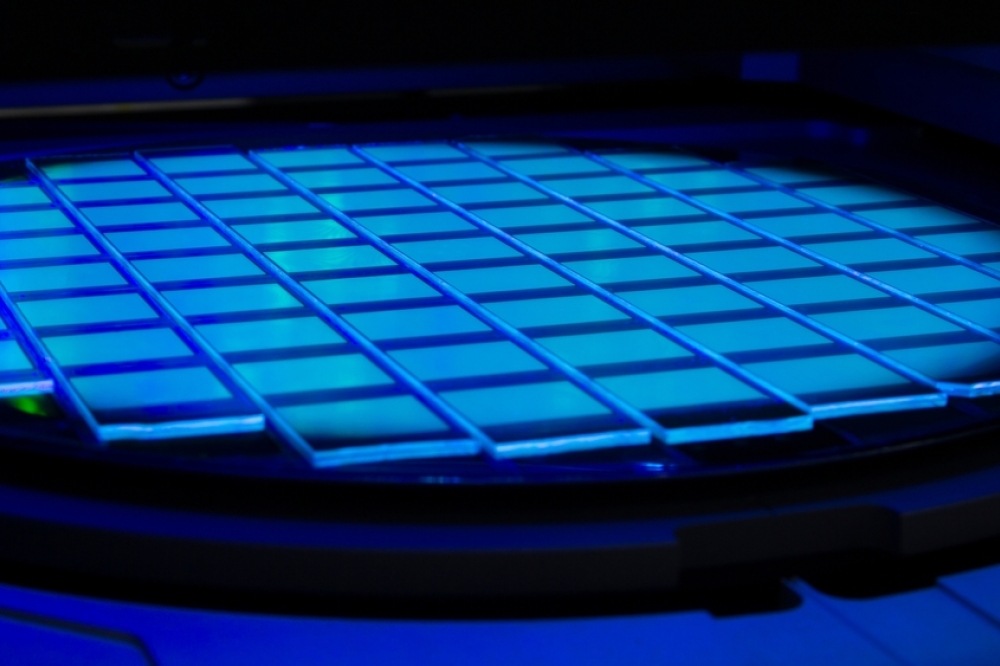
EUV lithography is the most sophisticated semiconductor manufacturing process in the world. Micron’s integration of EUV into its next node will play a key role in allowing the node to deliver faster, more power-efficient and higher-performance memory products and will enable the company to further its relentless pursuit of industry-first memory innovation.
“Micron is the only company that manufactures DRAM in Japan and is critical to setting the pace for not only the global DRAM industry but our developing semiconductor ecosystem,” said Satoshi Nohara, METI Director-General of the Commerce and Information Policy Bureau. “We are pleased to see our collaboration with Micron take root in Hiroshima with state-of-the-art EUV to be introduced on Japanese soil. This will not only deepen and advance the talent and infrastructure of our semiconductor ecosystem, it will also unlock exponential growth and opportunity for our digital economy.”
Micron’s 1-gamma node follows the company’s industry-leading 1-beta node which Micron began shipping samples of last November to mobile manufacturers. Cementing this industry-first leadership, the company has now started shipping its 1-beta-based LPDDR5X memory made in Hiroshima to industrial, automotive and consumer customers across Asia, the U.S. and Europe. The memory delivers low power and performance for AI, intelligent vehicles and virtual reality.
Micron’s multiple sites in Japan, including its fab in Hiroshima, are central to its research and development roadmap — and mass production — for Micron’s cutting-edge DRAM technology across its product lines. With more than 4,000 engineers and technicians in Japan, Micron is committed to advancing workforce development and the semiconductor ecosystem in Japan and, over the past five years, has hired more than 1,500 new employees in Japan. Micron supplies approximately one-third of the DRAM Japan uses in critical industries ranging from automotive to medical equipment, data centers and 5G infrastructure. With the smallest cell size in the world, the forthcoming 1-gamma technology will pave the way for mass production of sophisticated products required in complex applications from critical infrastructure to image processing networks.


