
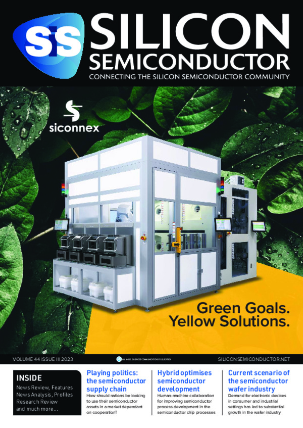
Green Goals. Yellow Solutions.
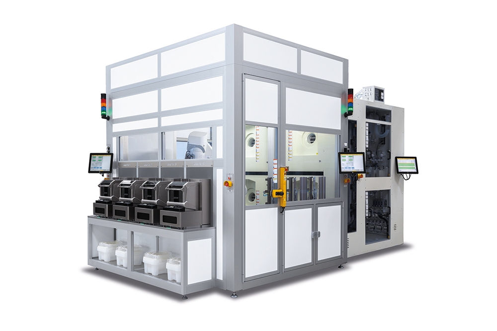
Sustainability and environmental health are in our DNA. BATCHSPRAY®
technology delivers energy-, media- and water-saving processes
throughout the chip manufacturing cycle. With two decades of experience
in batch spray and its hardware, Siconnex has grown to be the leading
supplier of sustainable wet processing equipment.
The production of semiconductors consumes a considerable amount of resources. By embracing sustainable products and processes, the semiconductor industry can mitigate its environmental impact and work towards a more sustainable future. Siconnex has been dedicated to efficient and resource-saving solutions for years, with its BATCHSPRAY® technology leading the way.
The company continuously enhances its expertise in sustainable processes, driven by both its own mission statement and the sustainability goals of its customers. One such advancement is the perc™ process for Post Etch Residue Clean, which represents our latest sustainable offering.
Big challenge: Polymer removal
“My experience with perc™ is that after sending wafers through several dry etch steps, we successfully found a recipe to remove all polymers and achieve better sidewall roughness. After conducting electrical checks, we even discovered improved performance compared to the existing process. I genuinely appreciate the excellent cooperation and collaborative work with Siconnex to find solutions for both new and existing processes.”
The statement by Dr. Julien Ladroue, STMicroelectronics, highlights the successful implementation of perc™ in addressing the challenge of polymer removal and achieving improved performance in chip production. In the context of device scaling and the difficulties associated with removing polymers using solvent-based processes, perc™ offers a solution that avoids the need for additional solvent media.
perc™, the process innovation from Siconnex, is specifically designed for Post Etch Residue Clean. This innovative application allows for the removal of several types of polymers by adjusting the process recipe. Siconnex’s unique spiking technology ensures that only a limited quantity of acid is required within the DIW stream, resulting in a significant reduction in acid flow.
In addition to polymer removal, the perc™ process provides the ability to control metal loss within the recipe. This brings numerous advantages, including guaranteed polymer removal, reduced metal loss, considerable reduction in chemical consumption and water usage, efficient waste treatment, and other benefits.
Overall, perc™ represents a significant advancement in chip production, offering a sustainable and efficient solution for polymer removal and contributing to the overall goal of achieving more sustainable and cost-effective processes.

After dry etch process (left) and after perc ™ process (right) Image Courtesy of STMicroelectronics
Polymer removal with Post Plasma Dicing Clean
Post Plasma Dicing Clean
Plasma etching for wafer dicing is a dry etch process that is becoming increasingly significant and will have a growing impact on the industry in the future. This approach offers the advantage of saving considerable space in the planar direction of dicing, while also minimizing residues compared to mechanical or laser dicing.
However, there are challenges associated with plasma etch dicing. Thicker top photoresists become more difficult to remove after treatment, and the removal of sidewall polymers becomes even more complex since the wafer is already diced.
To address these challenges, Siconnex has developed a process called Post Dicing Clean, which effectively removes polymers, photoresist, and residues in a single process step. By treating the entire frame and sticky tape where the diced wafer is positioned, the post dicing clean efficiently removes polymers from the sidewalls.
Additionally, plasma-treated photoresist can be easily removed, and residues can be cleaned from the surface.
The post dicing clean process effectively mitigates the drawbacks associated with plasma dicing, providing a sustainable and environmentally friendly solution. The technology used to handle these frames has been in operation for several years, ever since Siconnex initially delivered systems for fully automated 300 mm fabs.

Excellence in 300 mm wafer processing
Wet etch and clean processes performed in batch spray systems have long been essential in 200 mm fabs. However, the assumption that what works for 200 mm may not be applicable to 300 mm is incorrect. The results achieved in 300 mm wafer processing are equal with those achieved in 200 mm.
Traditional wet processes conducted in wet benches or single wafer tools, which have been in use for many years, have not delivered leading-edge results concerning within-wafer uniformity, wafer-to-wafer uniformity, batch-to-batch uniformity, cleanliness, and sustainable execution.
Siconnex’s BATCHSPRAY® equipment can significantly enhance all these specifications and more. Multiple processes can be performed within a single system, eliminating the need for multiple tools. Complex process sequences, such as AlSiCu etch followed by Freckle etch to remove any remaining silicon grains, and then a barrier etch to etch materials like Ti, TiN, TiW, and W, along with subsequent photoresist strip, can all be accomplished in one system. Furthermore, even dry etch processes, like the barrier etch mentioned earlier, can be replaced and executed sustainably.

Uniformity in batch processing of 300 mm wafers
With its fully automated BATCHSPRAY® systems, Siconnex provides leading-edge results for wet processing, making it an ideal match for the 300 mm wafer world. Siconnex offers a complete platform of hardware and processes for sustainable 300 mm wafer manufacturing. Through the development of new sustainable processes and the delivery of cutting-edge results for wet processing, Siconnex has experienced rapid growth in its installed base.

Process flow examples for Al etch, barrier etch and photostrip resist
With a focus on sustainability and continuous innovation, Siconnex is at the forefront of semiconductor manufacturing. The perc™ process addresses the challenge of polymer removal, while the Post Dicing Clean process tackles the complexities of plasma etching. The BATCHSPRAY® technology offers exceptional results for wet processing in 300 mm fabs, promoting uniformity, cleanliness, and sustainability. Siconnex’s commitment to developing new, sustainable processes contributes to a more sustainable and efficient future for the industry.
Benefits of perc™ process
Metal loss:
• Aluminum-Copper: <20 Å
•Titanium-Nitride: <15 Å
•No loss of Silicon-Oxide
Throughput per chamber:
•136 wph
•Process time: 21 min
Chemical consumption:
•DIW: 110 liters
•H2SO4: 100 ml
•H2O2: 700 ml
•HF: 70 ml
Advantages:
•Adjustable for each polymer
•Flexible parameter adjustment
•Very low chemical usage
•Point-of-use media usage
•Stable media concentration
•Open process time
•Single-use media
•Recontamination is avoided
•High throughput
•Solvents are obsolete
•Easy waste treatment
•4 chamber system available
•25W/50W chamber
•Available for 2“ - 12“ wafers


