
200 gigabits per second
Imec’s new SiGe BiCMOS optical receiver allows to process ever-increasing amounts of datacenter traffic.
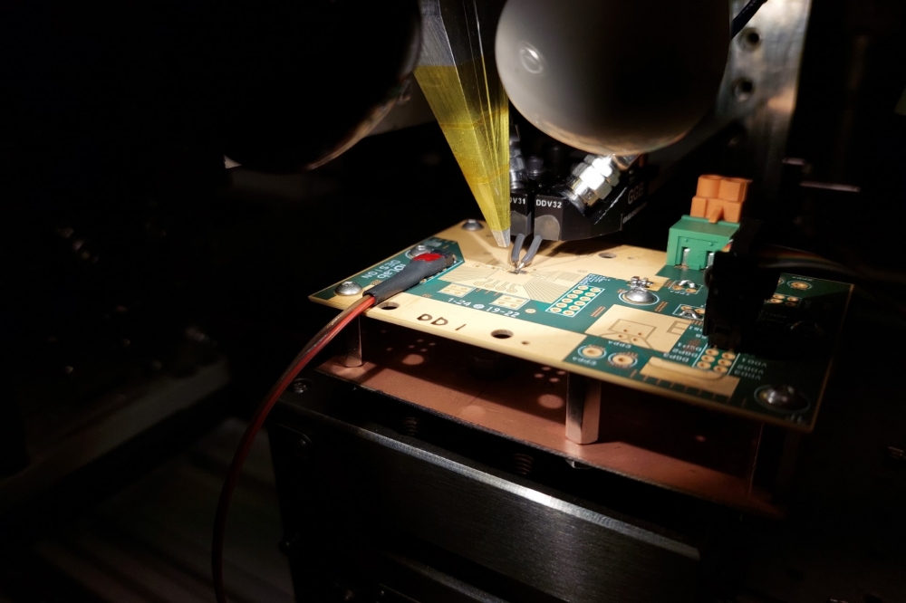
At the European Conference on Optical Communication (ECOC) taking place in Glasgow this week, a team of researchers from IDLab, an imec research group at Ghent University, Belgium, presents an optical receiver achieving a gross data rate of 200 Gbps. Their approach, combining a SiGe BiCMOS traveling-wave electronics integrated circuit and a Silicon Photonics Germanium photodetector, offers not only speed but also scalability, two prerequisites if we want to meet exploding data-rate needs.
The need for speed
From artificial intelligence to cloud computing and 5G: data-intensive applications are finding their way into different industries and many aspects of our daily lives. To keep up with today’s and especially tomorrow’s data-processing demands, data centers will need optical communication networks that perform at higher and higher speeds.
“Currently, the most performant optical datacom transceivers operate at speeds up to 800 Gbps, using for example 8 x 100 Gbps channels, but the field is envisioning doubling the channel capacity to 200 Gbps to reduce the transceiver complexity, cost and power consumption while improving manufacturing yield,” says Peter Ossieur, program manager for high-speed transceivers at imec’s IDLab and professor at Ghent University.
Fast and scalable
Ossieur is leading a team of researchers working towards high-speed integrated circuits for photonics applications. His team has now achieved a gross data rate of 200 Gbps by co-integrating a traveling-wave SiGe BiCMOS transimpedance amplifier with a silicon photonics Ge photodetector.
Aside from the speed, the use of mainstream SiGe BiCMOS makes the technology more scalable and therefore affordable. “An alternative to reach such speeds are InP electronics, which is a more expensive and less scalable technology,” says Ossieur. “SiGe BiCMOS allows us to integrate more functionalities and the chips can also be manufactured at higher volumes.”
The next generation
If optical transceivers are to keep up with exploding data rates, all building blocks need to handle higher speeds. The team demonstrates their result in a setup with a silicon photonics Ge photodetector from imec’s integrated silicon photonics platform (iSiPP), targeted to the telecom, datacom and medical diagnostics industries.
Joris Van Campenhout, fellow and program director optical I/O at imec, says the new optical receiver represents one of the many steps imec is taking to ready its silicon photonics platforms for demanding 200Gbps-and-beyond applications:
“These latest results represent one more data point showcasing the capability of imec’s silicon photonics platform (iSiPP) to operate at lane rates of 200Gbps, a key requirement for upcoming pluggable and co-packaged optics. .”
The work received support through European Union’s Horizon 2020 projects POETICS (No 871769) and NEBULA (No 871658) and will be presented at the European Conference on Optical Communication.


