
AP&S shines with innovative NexAStep at SEMICON Europa & trains in its own academy
The semiconductor industry has made enormous strides in recent decades
and plays a critical role in our modern world. A key component for the
production of high-quality semiconductor devices is wet process
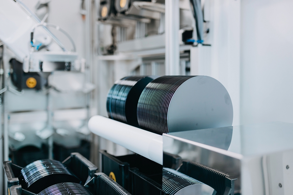
equipment. These systems have been built by AP&S for 20 years and
are essential for cleaning and treating wafers. The latest development
from the company is the NexAStep wet bench, which is used for batch
processing.
THE COMPACT SYSTEM DESIGN here represents a fundamental advancement that allows optimal use of the clean room, as the system takes up less space. The efficient arrangement of chemical supply, drains, receiver tanks and control cabinets in the module footprint further reduces space requirements and facilitates access for maintenance and operation. The modular plant design allows the plant to be quickly assembled, disassembled and reconfigured, increasing flexibility in production. This allows companies to quickly adapt to market changes when necessary and scale the plant to expand production capacity if necessary.

Wet bench NexAStep – Our new Batch Tool for high throughput Wet Processing
An integrated axis at the front of the NexAStep minimizes particle generation and simplifies direct access. Visually, a signal light integrated into the paneling provides 180-degree visibility for improved access and safety.
With its sister company tepcon GmbH, AP&S has a software company at its side that, among other things, assisted in the implementation of a user-friendly intuitive HMI. The simplified operation of the system, optimized monitoring and efficient control were the main focus here. This ensures efficient process control.
“In the area of condition monitoring, our solutions offer configurable visualization of real-time data in tables, graphs or flowcharts, monitoring of limit values and very timely alarming via email, SMS or WhatsApp. The customer can intervene flexibly at any time and from anywhere via his mobile device. Machine failures can be avoided in real time. The analysis of process data enables the recording and tracking of recipes. Operating errors become visible through comparison with historical data, which leads to optimization of recipe processes and efficient planning of service calls,” explains Christoph Kluge, Managing Director of tepcon GmbH.

Up to 75 storage locations guarantees an uninterrupted production flow
High throughput due to automatic control and loading also played an important role in the choice of technology. By using an OHT (Overhead Hoist Transport), the system can be integrated into existing complex process chains, thereby accelerating the transport of carriers loaded with wafers. The resulting integrated warehouse in the wet process system with its up to 75 storage locations guarantees an uninterrupted production flow.
The up to 12 LMC process carriers are thus supplied without interruption with 100 wafers/halfpitch (8 inches) each, which supports an uninterrupted and targeted production flow. Thus, AP&S doubled troughput on the same footprint and significantly reduce TCO (same chemistry twice the throughput).
“With the new NexAStep plant platform, we have been able to combine all the positive experience that we have built up as AP&S over the past 20 years with current customer and market requirements in one plant. The next level of “automation, throughput and functionality” in wet process plant engineering could be climbed. It fills us with pride to be able to generate data in the field with the first plants and to see the added value that the new concept represents for us and the customers,” says Tobias Bausch (CMO&CTO).

Highly dynamic axis system for wafer-friendly transport and fast empty runs
The wet process plants of the future use a combination of established drying processes such as the Marangoni effect and NID hot drying (Nitrogen IPA Dispense-Drying). Both processes are examples of specialized drying techniques that have already found their proven and qualified application for various diverse semiconductor technologies.
In order to give customers as much freedom as possible in designing the filling and process recipes, these can be precisely programmed individually and selected depending on the product.
Further innovations of the NexAStep system are the optimized extraction of the process chamber and the resulting lower contamination as well as the high process temperature of up to 170°C, which allows a higher process speed.
Overall, these advanced wet process systems offer the semiconductor industry significant added value for customers. They enable more efficient, more flexible, more cost-optimized, more automated and higher-quality production of semiconductor components, thus contributing to the further development of the technology sector.

Manual operation and loading possible for maximum flexibility
This is precisely what the AP&S Academy, which opened its doors in June of this year, also supports.
“We have been successfully conducting training courses at customers’ on-site semiconductor factories for a long time. In recent years, however, demand here has grown significantly. There were also increasing calls from customers for a central training center for wet process technology so that running production facilities would not be affected by training purposes. This coincided with our strategy for founding the AP&S Academy,” explains COO and initiator of the AP&S Academy Tobias Drixler.
Steffen Hölderle (Head of Service) and André Menge (Senior Service & Training) were proudly presented with the key to the AP&S Academy. Managing Director Tobias Drixler (COO) sees the training center as a platform for preparing both new employees and customers individually and specifically for the respective uses of the machines. The interest in such training offers has increased enormously due to the current shortage of skilled workers and the need to adequately instruct and thus qualify non-specialist personnel in the world of chemical wet process technology.

From left to right: Managing Director Tobias Drixler (COO), Steffen
Hölderle (Director of Service) and André Menge (Senior Service &
Training)
Four training modules, which can be attended continuously, are offered by the company’s employees, who have both the knowledge of the semiconductor industry and the pedagogical skills. The know-how of the employees of AP&S International GmbH, which has been accumulated over 20 years, is thus passed on to interested parties in a focused manner in order to teach the handling of wet process equipment in a practice-oriented manner.
Shareholder and Managing Director Alexandra Laufer-Müller: “Our goal is to cover the entire spectrum of wet process solutions required in both the front-end and back-end production chains. For example, our products perform functions such as cleaning, etching, metal etching, PR strip, electroless plating, lift-off, drying and development processes. This is the beginning. Together with our customers, we are constantly developing new outstanding processes, such as the AP&S metal lift-off process, which is unique in today’s market. We also offer manual, semi-automatic and fully automatic applications.”
Alexandra Laufer-Müller (Shareholder & CEO)
Tobias Bausch (CMO&CTO)

Christoph Kluge (Managing Director tepcon GmbH)


