
AI boom provides SUSS MicroTec with record orders for temporary bonders
SUSS MicroTec's temporary bonding solutions enable rapid expansion of AI applications and let production in Taiwan grow.
SUSS MicroTec, a leading manufacturer of equipment and process solutions for the semiconductor industry, plays a key role in the production of the high-performance microchips required for AI applications with its solutions for temporary wafer bonding. Accordingly, the company's order books are currently full: Between June and the end of October 2023, SUSS MicroTec has booked orders worth around EUR 100 million for temporary bonding solutions for AI applications – never before has the demand for bonders been greater.
SUSS MicroTec has been a leading provider of temporary bonding solutions for around ten years. The strategic development of expertise in temporary bonding over many years is currently giving the company a 'decisive advantage'. Markus Ruff, Head of Bonding Solutions, explains: "The enormous interest in generative AI has taken the global market by surprise. Chip manufacturers now have to meet the demand for AI chips as quickly as possible. To do this, they need our temporary bonding solutions, as these have already been perfectly matched to their processes and qualified by them. We are therefore growing in step with the massive increase in capacity."
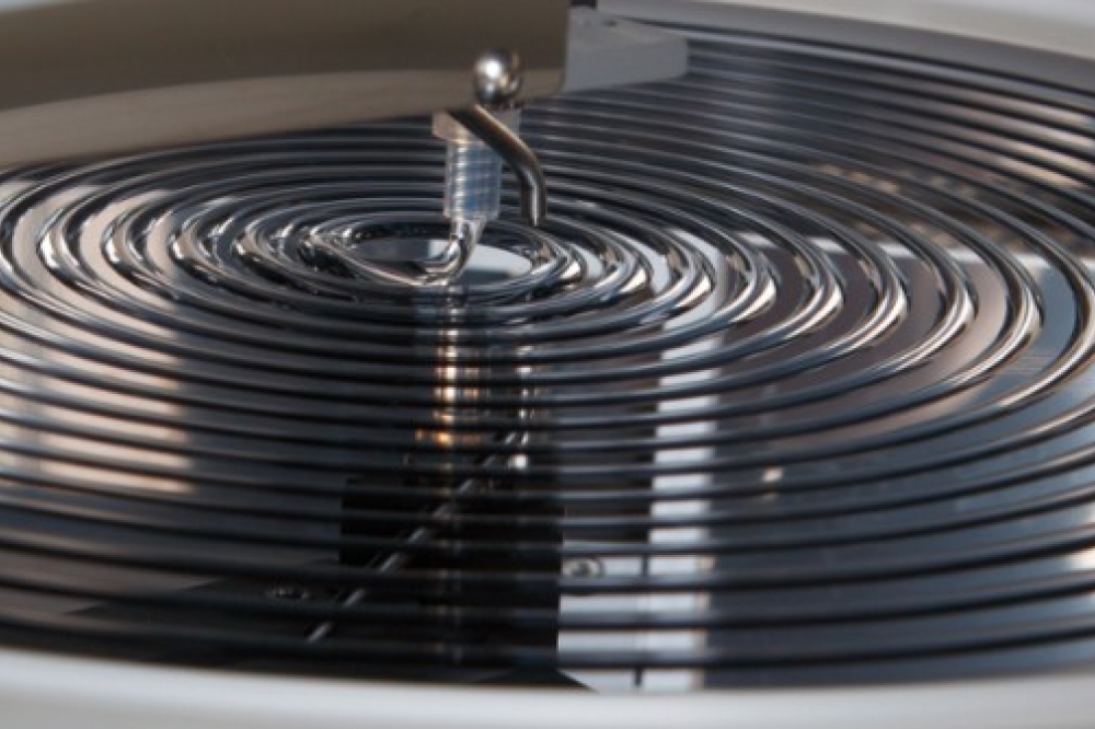
An AI chip consists of one or more logic chips and one or more high-performance memory chips, so-called HBMs (high bandwidth memory). In the manufacturing process of AI chips, temporary bonding solutions are indispensable for two steps. HBMs must be ground as thin as possible. For the grinding process and further processing, the wafer must be reinforced by temporarily bonding it to a second wafer. Afterwards, the bond can be released again by debonding. The wafer must then be cleaned of adhesive residues. With the XBS300 and XBC300 bonding platforms, SUSS MicroTec offers efficient solutions for all three sub-processes.
In addition, temporary bonding solutions from SUSS MicroTec are used by one of the world's leading foundries in advanced packaging. There, logic chip(s) and memory chip(s) are coupled together to enable the fastest and most powerful communication possible between the chips. In this packaging process, the temporary bonding solution does not connect two wafers together, but performs pressure annealing, which straightens the carrier wafer.
To meet high customer demand, SUSS MicroTec is currently expanding production capacity at its production site in Hsinchu (Taiwan). In the future, the XBS300 temporary bonder will be manufactured there. Preparations for this are in full swing: more than 50 new employees are being hired for the Hsinchu site. Teams from Taiwan are currently undergoing intensive training in Sternenfels (Germany). Dr. Thomas Rohe, Chief Operating Officer of SUSS MicroTec, comments: "We want to be a reliable and flexible partner for our customers in the long term. This requires us to be able to quickly adapt our production capacities to market developments. We are now taking this step with the short-term expansion of production in Hsinchu." The site in Taiwan will grow to over 300 employees in the coming months. Up to twelve bonders per year are to be manufactured there in future. To date, coating solutions and the DSC300 UV projection scanner have been manufactured in Hsinchu.


