+44 (0)24 7671 8970
More publications     •     Advertise with us     •     Contact us
 
Loading...
News Article

Earthquake temporarily halts Japan facilities
News


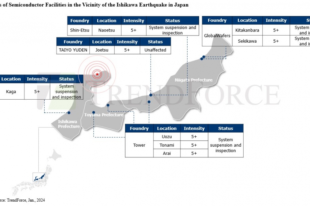
TrendForce’s investigation into the impact of the recent strong earthquake in the Noto region of Ishikawa Prefecture, Japan, reveals that several key semiconductor-related facilities are located within the affected area.

This includes MLCC manufacturer TAIYO YUDEN, silicon wafer (raw wafer) producers Shin-Etsu and GlobalWafers, and fabs such as Toshiba and TPSCo (a joint venture between Tower and Nuvoton).

Given the current downturn in the semiconductor industry and the off-peak season, along with existing component inventories and the fact that most factories are located in areas with seismic intensities of level 4 to 5—within the structural tolerance of these plants—preliminary inspections indicate no significant damage to the machinery, suggesting the impact is manageable.

In terms of silicon wafer production, Shin-Etsu and GlobalWafers' facilities in Niigata are currently shut down for inspection. The crystal growth process in raw wafer manufacturing is particularly sensitive to seismic activity. However, most of Shin-Etsu's crystal growth operations are primarily in the Fukushima area, thus experiencing limited impact from this earthquake. SUMCO reported no effects.

On the semiconductor front, Toshiba's Kaga facility in the southwestern part of Ishikawa Prefecture is currently undergoing inspections. This site includes a six-inch and an eight-inch factory, along with a twelve-inch facility slated for completion in the 1H24. Additionally, the three TPSCo factories in Uozu, Tonami, and Arai—co-owned by Tower and Nuvoton (formerly Panasonic)—are all undergoing shutdowns for inspections. In contrast, USJC (UMC's acquisition of the Mie Fujitsu plant area in 2019) was not affected.

MLCC manufacturer TAIYO YUDEN’s new Niigata plant, designed to withstand seismic activity up to level 7, reported no equipment damage. Murata (MLCC fabs only) and TDK’s MLCC plants experienced seismic intensities below level 4 and were not notably affected. However, Murata’s other factories (Non-Production MLCC) in Komatsu, Kanazawa, and Toyoma, which are in the areas with seismic intensity above 5, were closed for the New Year holiday, and staff are currently assessing any damage.

Reality AI Explorer Tier offers free AI/ML development access
AEM introduces new generation of Automated Burn-In Systems
NPUs are emerging as the main rival to Nvidia’s AI dominance, says DAI Magister
Camtek receives a $20M order from a Tier-1 OSAT
Free samples of every STMicroelectronics NPI IC available from Anglia
NY CREATES and SEMI sign MoU
Major government investment to 'propel' Canada
QuickLogic announces $5.26 million contract award
ASNA and Athinia collaborate
Global sales forecast to reach record $109 billion in 2024
AMD to acquire Silo AI
Nanotronics unveils 'groundbreaking' Gen V AI Model
Aitomatic unveils SemiKong
Biden-Harris Administration reveals first CHIPS for America R&D facilities and selection processes
Collaboration to produce cutting-edge AI accelerator chips
Oxford Ionics breaks global quantum performance records
Adeia wins ECTC Award for paper on “Fine Pitch Die-to-Wafer Hybrid Bonding”
AEM introduces new generation of Automated Burn-In Systems
Sydney council forges vital semiconductor agreement
EV Group's EVG880 LayerRelease wins 2024 Best of West
Biden-Harris Administration to invest up to $1.6 billion
Cyient sets up subsidiary for semiconductor business
EMD Electronics network leaders honoured
Accenture acquires Cientra
Introducing Park FX200
Deep learning chipset market to surge to $72.8 billion by 2033
PI Innovation Award 2024: Nanobodies for Diagnostic and Therapeutic Applications
Graphcore joins Softbank Group
Kaman Measuring highlights high precision displacement sensors
Si2 reveals recipients of Annual Power of Partnerships Award
Advantest achieves ASPICE Level 2 Certification for V93000 SmarTest 8 Software
Semiconductors to become a trillion-dollar industry by 2030
×
Search the news archive

To close this popup you can press escape or click the close icon.
Logo
×
  • 1st January 1970
  • 1st January 1970
  • 1st January 1970
  • 1st January 1970
  • 1st January 1970
  • 1st January 1970
  • 1st January 1970
  • 1st January 1970
  • View all news 22645 more articles
Logo
×
Register - Step 1

You may choose to subscribe to the Silicon Semiconductor Magazine, the Silicon Semiconductor Newsletter, or both. You may also request additional information if required, before submitting your application.


Please subscribe me to:


You chose the industry type of "Other"

Please enter the industry that you work in: