
Imec presents levers to reduce the CO2 equivalent footprint of lithography and etch
Process simplification, dose reduction, improved material stacks for etching, and recipe optimization are key knobs towards reduced emissions.
This week, at the 2024 Advanced Lithography + Patterning Conference, imec presented an overview of advanced node lithography and etch related processes that contribute the most to direct emissions of CO2. Also, more sustainable patterning directions are proposed, including, for example, opportunities for dry etch processes and process simplification.
Semiconductor devices fabricated in 2021 have a CO2 equivalent footprint of about 175 megatonnes, equivalent to the yearly emissions associated with about 30 million people. Using imec.netzero, a virtual fab model developed in the frame of imec’s Sustainable Semiconductor Technologies and Systems (SSTS) program, imec showed that together, lithography and etch contribute over 40% of advanced logic node Scope 1 and Scope 2 emissions.
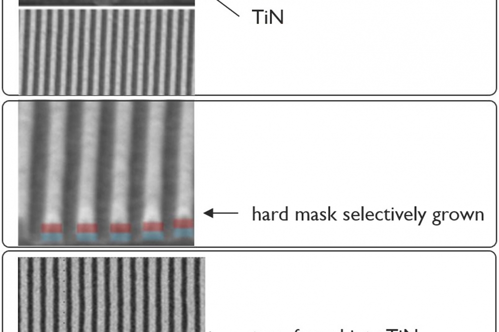
Emily Gallagher, a principal member of the technical staff at imec: “There are important levers available to reduce that impact. For example, most dry etch processes rely on fluorinated compounds that have very high global warming impact, and direct emissions associated with those processes are high. To minimize their consumption and thus reduce their impact, we present process and design directions for future patterning enabling ultra-thin resists and underlayers, minimal passivation and low process temperatures for etch. Using these principles, we demonstrated a High-NA-compatible metal line etch process step that has ~6% of the process gas emissions relative to the reference process before abatement.”
For lithography, the larger challenge are the emissions associated with generating electricity. Consequently, the levers are using greener energy, reducing the number of multi-patterning steps, reducing photoresist dose, and enhancing scanner throughput. Emily Gallagher: “If an EUV scanner’s throughput is reduced by 20% and the impact is modeled with imec.netzero through the full process of an advanced logic node wafer, we achieve over 6% more Scope 2 emissions (energy component). In addition, replacing one EUV low-NA litho-etch-litho-etch (LELE) via process module with the High-NA EUV single exposure equivalent can reduce emissions by about 30%; this reduction is achieved by eliminating process steps and despite the increase in power consumption associated with the High-NA scanner’s advanced stages and drive laser.”
“Sustainability is important for imec and we are pleased to see that it is also gaining importance at the SPIE Advanced Lithography and Patterning conference,” adds Emily Gallagher. “An informal search of papers shows a promising trend: in 2018 there was only one paper that mentioned sustainability and now, only six years later, the conference is anticipating 45 papers in the sustainability track, four of them coming from imec. Last year shattered global climate records, so it
is essential that we all take action as organizations and as individuals. Imec has embraced this action at all levels including our research.”


