
Lightning Mode added to QUADRA metrology system
Lightning Mode boosts image acquisition speed 160-fold over current automated AFM metrology.
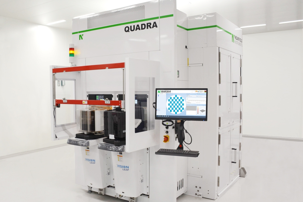
Nearfield Instruments has launched “Lightning Mode™”, a new feature for QUADRA®, which is the semiconductor industry’s highest-throughput atomic force microscopy (AFM) metrology system for advanced semiconductor devices. QUADRA is now fully qualified and deployed for high-volume manufacturing (HVM) at the industry’s leading fabs.
QUADRA is a high-throughput, in-line scanning probe metrology system with groundbreaking multi-miniaturized AFM head architecture to enable on-device, non-destructive three-dimensional (3D) metrology. It accelerates time-to-yield and HVM yield optimization and control in memory (VNAND, DRAM, HBM) and logic processes, including high-aspect-ratio structures as well as hybrid bonding applications and (high-NA) EUV resist structures.
QUADRA, combined with the new Lightning Mode, boosts productivity with a more than 160-fold increase in image acquisition speed when benchmarked against existing state-of-the-art automated AFM systems. The extremely high throughput of QUADRA, along with its superior accuracy, enables customers non-destructively to determine lot-to-lot, wafer-to-wafer and intra-wafer process variations in full 3D with very high wafer and lot coverage.
“Hybrid bonding is a critical technology to support the future demands for computational power, which is driving more chip stacking and increased data transmission; more efficient energy consumption in multi-chip systems is a key. Hybrid bonding plays a crucial role in artificial intelligence (AI) chip systems, both in 3D packaging and new-generation high-bandwidth memory (HBM) manufacturing. However, it comes with additional complexity to 3D packaging and chiplets, increasing the importance of angstrom-level, non-destructive metrology with the capability of not only die-to-die, but also pad-to-pad metrology, which has historically demonstrated limited throughput over the more conventional techniques like AFM,” said Hamed Sadeghian, CEO, Nearfield Instruments. “QUADRA is transforming semiconductor production metrology, and especially now with our new Lightning Mode – the only metrology system capable of providing highly accurate, in-line, non-destructive 3D measurements with extremely high throughput on advanced technology nodes. It is validated and qualified for all device and package types in the fab.”
QUADRA is now fully validated for measuring dense structures with high aspect ratios on advanced DRAM and logic devices. Nearfield Instruments anticipates growing demand, especially with its new Lightning Mode that provides the fastest imaging speed of any in-line AFM metrology system in the world, supporting massive metrology needs. “We anticipate multiple orders of the QUADRA system by the end of 2024,” Sadeghian added.
Nearfield Instruments’ product portfolio also includes the AUDIRA® system, which provides highly accurate and reproducible nanometer-level measurements of buried features and defects, such as voids, in advanced memory and logic devices. AUDIRA uses an acoustic approach that is fast, very precise and non-destructive, with the added advantages of being in-line with a fast turnaround time.


