Imec achieves breakthrough in silicon photonics
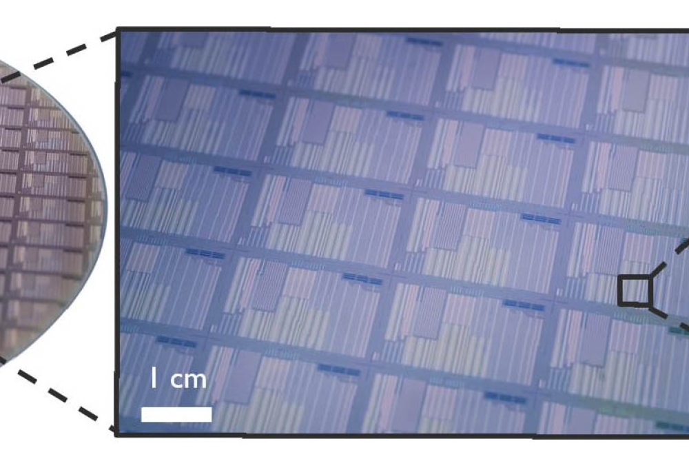
First full wafer-scale fabrication of electrically-pumped GaAs-based nano-ridge lasers on 300 mm silicon wafers.
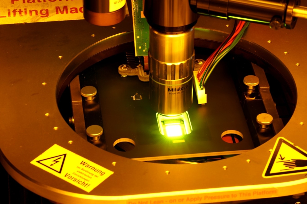
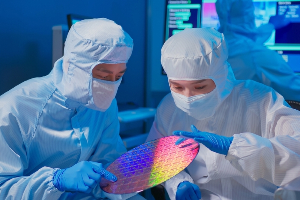
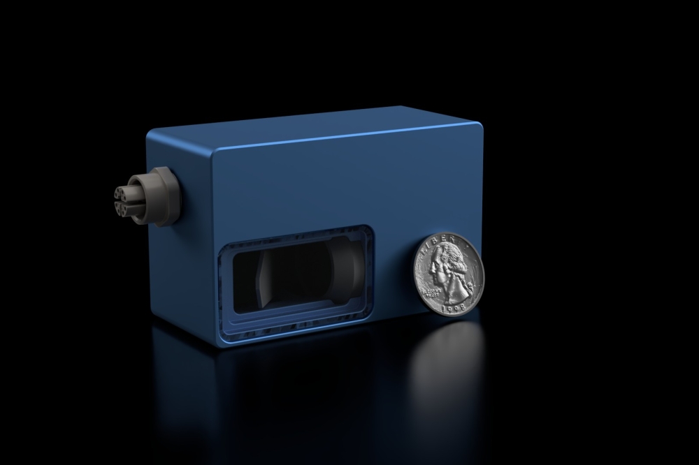
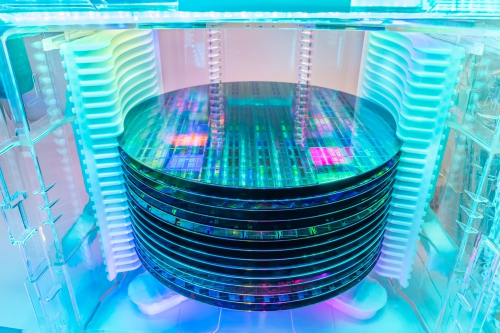
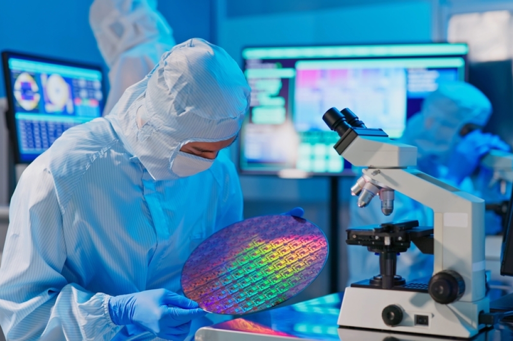
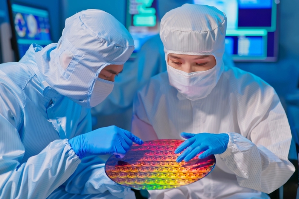
Imec has announced a significant milestone in silicon photonics with the successful demonstration of electrically-driven GaAs-based multi-quantum-well nano-ridge laser diodes fully, monolithically fabricated on 300 mm silicon wafers in its CMOS pilot prototyping line. Achieving room-temperature continuous-wave lasing with threshold currents as low as 5 mA and output powers exceeding 1 mW, the results, detailed in last week’s Nature publication, demonstrate the potential of direct epitaxial growth of high-quality III-V materials on silicon. This breakthrough provides a pathway to the development of cost-effective, high-performance optical devices for applications in data communications, machine learning and artificial intelligence.
The lack of highly scalable, native CMOS-integrated light sources has been a major roadblock for the widespread adoption of silicon photonics. Hybrid or heterogeneous integration solutions, such as flip-chip, micro-transfer printing or die-to-wafer bonding, involve complex bonding processes or the need for expensive III-V substrates which are often discarded after processing. This not only increases costs but also raises concerns about sustainability and resource efficiency. For that reason, the direct epitaxial growth of high-quality III-V optical gain materials selectively on large-size silicon photonics wafers remains a highly sought-after objective.
The large mismatch in crystal lattice parameters and thermal expansion coefficients between III-V and Si materials inevitably initiates the formation of crystal misfit defects, which are known to deteriorate laser performance and reliability. Selective-area growth (SAG) combined with aspect-ratio trapping (ART) significantly reduces defects in III-V materials integrated on silicon by confining misfit dislocations within narrow trenches etched in a dielectric mask.
“Over the past years, imec has pioneered nano-ridge engineering, a technique that builds on SAG and ART to grow low-defectivity III-V nano-ridges outside the trenches. This approach not only further reduces defects but also enables precise control over material dimensions and composition. Our optimized nano-ridge structures typically feature threading dislocation densities well below 105 cm-2. Now, imec exploited the III-V nano-ridge engineering concept to demonstrate the first full wafer-scale fabrication of electrically pumped GaAs-based lasers on standard 300 mm silicon wafers, entirely within a CMOS pilot manufacturing line,” says Bernardette Kunert, scientific director at imec.
Leveraging the low-defectivity GaAs nano-ridge structures, the lasers integrate InGaAs multiple quantum wells (MQWs) as the optical gain region, embedded in an in-situ doped p-i-n diode and passivated with an InGaP capping layer. Achieving room-temperature, continuous-wave operation with electrical injection is a major advancement, overcoming challenges in current delivery and interface engineering. The devices show lasing at ~1020 nm with threshold currents as low as 5 mA, slope efficiencies up to 0.5 W/A, and optical powers reaching 1.75 mW, showcasing a scalable pathway for high-performance silicon-integrated light sources.
“The cost-effective integration of high-quality III-V gain materials on large-diameter Si wafers is a key enabler for next-generation silicon photonics applications. These exciting nano-ridge laser results represent a significant milestone in using direct epitaxial growth for monolithic III-V integration. This project is part of a larger pathfinding mission at imec to advance III-V integration processes towards higher technological readiness, from flip-chip and transfer-printing hybrid techniques in the near term, over heterogeneous wafer- and die-bonding technologies and eventually direct epitaxial growth in the longer term,” states Joris Van Campenhout, fellow silicon photonics and director of the industry-affiliation R&D program on Optical I/O at imec.