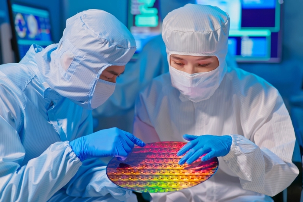
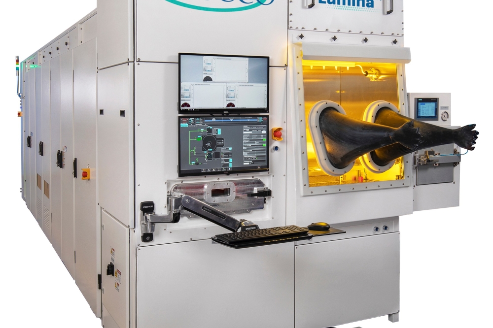
Soitec continues its collaboration with MIT's Microsystems Technology Laboratories
Soitec continues its research and membership agreement with MIT’s Microsystems Technology Laboratories. This agreement covers research in innovative semiconductor materials for diverse applications, including mobile communications, power devices, sensors and quantum computing.
Soitec is continuing its research collaboration with the Microsystems Technology Laboratories (MTL) of the Massachusetts Institute of Technology (MIT), further solidifying its presence in the North American semiconductor sector.
This initiative aims to diversify technological collaborations and anticipate the future needs of the industry.
In the United States, Soitec is intensifying its efforts amidst favourable industrial and regulatory dynamics supporting semiconductor development. In this respect, MIT plays a key role through its Microsystems Technology Laboratories (MTL), in which Soitec is now a member of the Industrial Advisory Board, which actively contributes to defining strategic research directions in microelectronics.
Christophe Maleville, Soitec’s Senior Executive Vice President in charge of Innovation and Chief Technology Officer, commented on the partnership: "The agreement between Soitec and MIT reflects a global strategy centred on excellence and impact. By joining forces with a world-renowned institution like MIT, Soitec gains unique access to cutting-edge technological advances and an exceptional innovation ecosystem. Combining innovation, technological expertise and regional ecosystem engagement, Soitec is reinforcing its position to do important research in the field"
Tomás Palacios, Director of MTL and Professor at MIT, added: “We are proud to have Soitec as a member of the MIT Microsystems Technology Laboratories. Soitec is a technology leader in the development and commercialization of advanced semiconductor substrates, and we are excited to be able to work closely with their team in the development of the next generation of semiconductor materials and devices.”
International Collaboration: The Cornerstone of Soitec's Innovation Strategy
Soitec collaborates with industrial innovation platforms, academic institutions and research centres, reflecting a long-term vision and a commitment to partnering with centres of excellence.
In Europe, Soitec has established strategic partnerships with institutions like Imec, Leti and Fraunhofer, enhancing its regional expertise and its deep understanding of client needs.
In Asia, Soitec has collaborated with organizations such as the Institute of Microelectronics of Singapore (IME) and the National University of Singapore (NUS) for years, with plans to expand its innovation activities to Japan, a key player in materials development.
Soitec is pursuing high-impact innovation projects in the United States, forming partnerships with key centres identified under the CHIPS Act and engaging with universities like UC San Diego and UC Riverside.
These initiatives span domains such as mobility, artificial intelligence and advanced packaging, underscoring Soitec’s ambition to remain at the forefront of technological advancements.