GlobalFoundries to create New York Advanced Packaging and Photonics Center
First of-its-kind center will offer advanced packaging and test capabilities in New York for U.S.-made essential chips used in AI, automotive, aerospace and defense, and other applications.
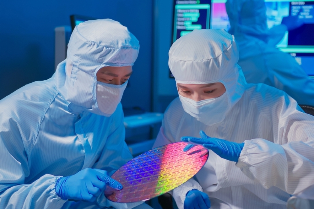
GlobalFoundries has announced plans to create a new center for advanced packaging and testing of U.S.-made essential chips within its New York manufacturing facility. Supported by investments from the State of New York and the U.S. Department of Commerce, the first-of-its-kind center aims to enable semiconductors to be securely manufactured, processed, packaged and tested entirely onshore in the United States to meet the growing demand for GF’s silicon photonics and other essential chips needed for critical end markets including AI, automotive, aerospace and defense, and communications.
Growth in AI is driving the adoption of silicon photonics and 3D and heterogeneously integrated (HI) chips to meet power, bandwidth and density requirements in datacenters and edge devices. Silicon photonics chips are also positioned to address power and performance needs in automotive, communications, radar, and other critical infrastructure applications. To meet this growing demand, GF’s New York Advanced Packaging and Photonics Center is expected to offer:
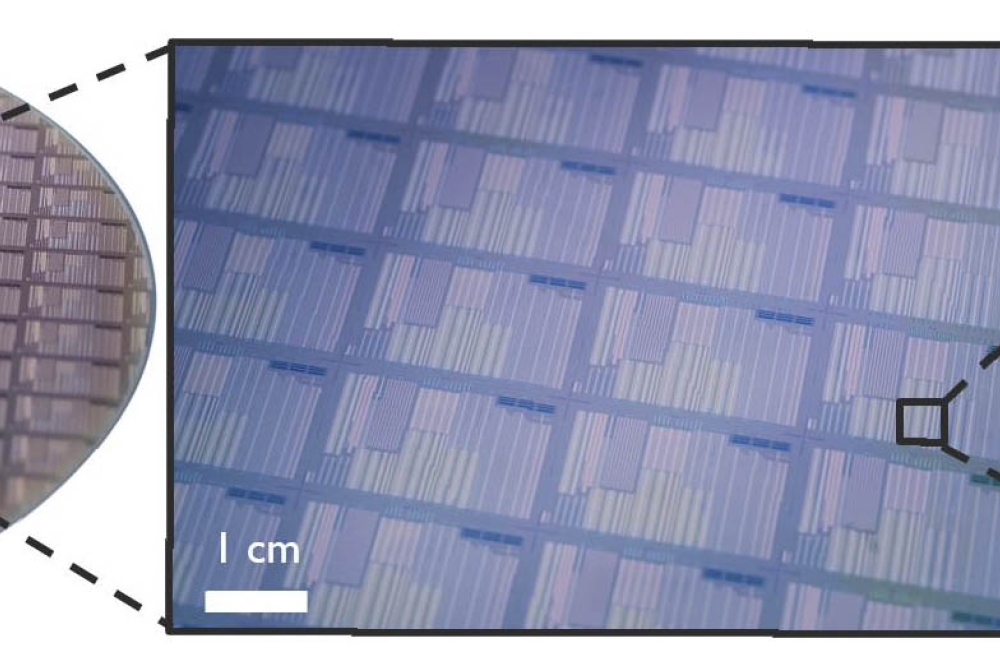
Advanced packaging, assembly and testing for GF’s differentiated silicon photonics platform, which brings together optical and electrical components on a single chip to realize power efficiencies and performance advantages.
Full turnkey advanced packaging, bump, assembly and testing for aerospace and defense customers under GF’s Trusted Foundry accreditation, allowing chips used in sensitive national security systems to never leave the U.S. during production.
New production capabilities for the advanced packaging, wafer-to-wafer bonding, assembly and testing of 3D and HI chips using GF’s 12LP+, 22FDX®, and other leading platforms.
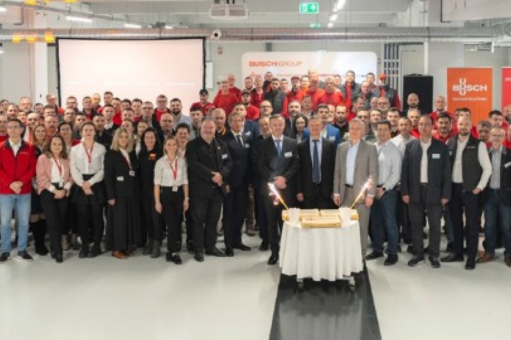
“We’re proud to partner at the state and federal level on this new center, which is a direct response to our customers asking for more geodiversity in their supply chains and additional support with advanced packaging solutions for GF silicon photonics, Trusted, and 3D/HI offerings,” said Dr. Thomas Caulfield, president and CEO of GF. “The New York Advanced Packaging and Photonics Center will be unique in our industry and will play a vital role in the continued growth of the Empire State’s world-class semiconductor manufacturing and innovation ecosystem.”
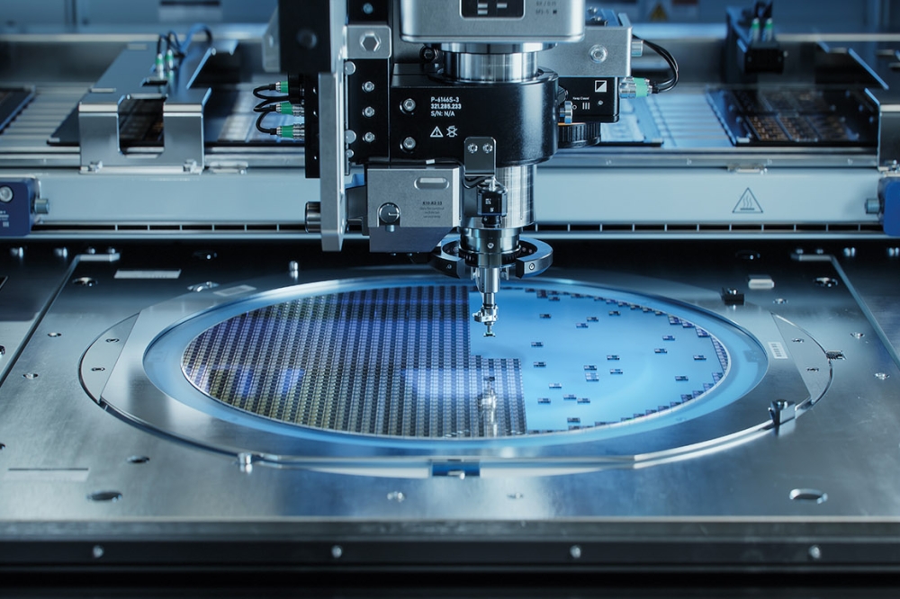
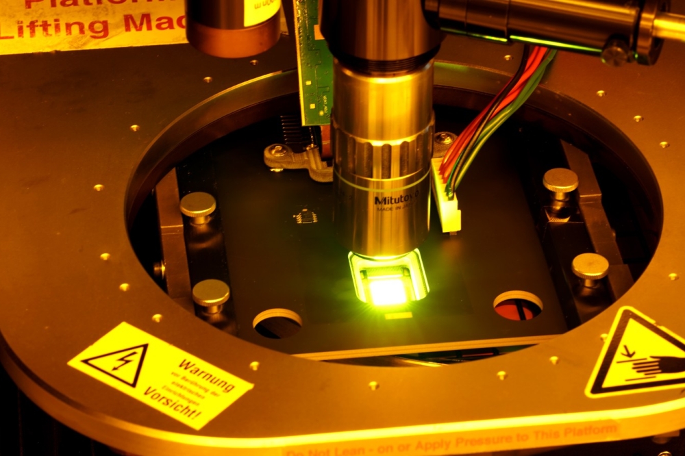
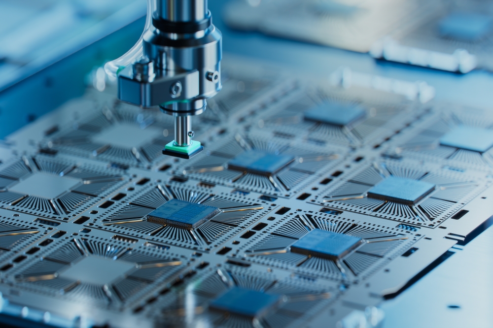
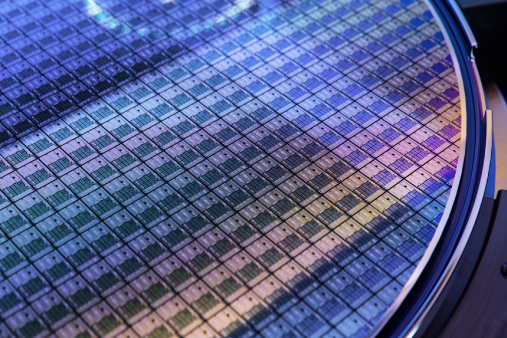
The New York Advanced Packaging and Photonics Center aims to expand GF’s advanced packaging capabilities – the process of transforming chips into individual packages ready for end-product use – to provide customers an end-to-end U.S.-based solution for chips made at GF’s New York manufacturing facility. Across the semiconductor industry, most advanced packaging today takes place in Asia.
GF’s overall investment in the New York Advanced Packaging and Photonics Center is expected to be $575 million, with an additional $186 million investment in research and development over the next 10-plus years. These efforts are expected to create approximately 100 new full-time GF jobs in New York over the next five years.
New York state will provide up to $20 million in new support for the new center, which is in addition to the previously announced $550 million in support for GF from the New York State Green CHIPS program. The U.S. Department of Commerce will provide up to $75 million in direct funding to support the center, supplementing the previously announced GF award under the CHIPS and Science Act.
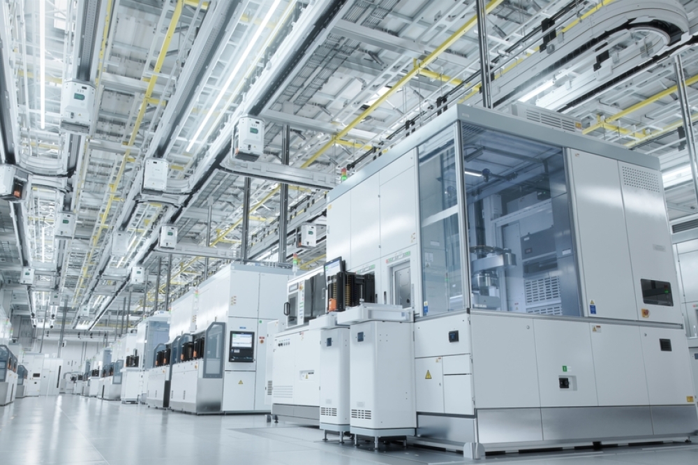
GF employs approximately 2,500 people at its Malta, New York, fab and has invested more than $16 billion in the facility since it opened in 2011. GF’s New York fab has Trusted Foundry accreditation and manufactures secure chips in partnership with the U.S. government.