Empowering semiconductor manufacturers to embrace new markets
Reduction of outgassing and elimination of contaminants is a pressing need for an industry spanning a wide variety of new markets.
By Jason Davis, New Business Development, Junkosha USA Inc.
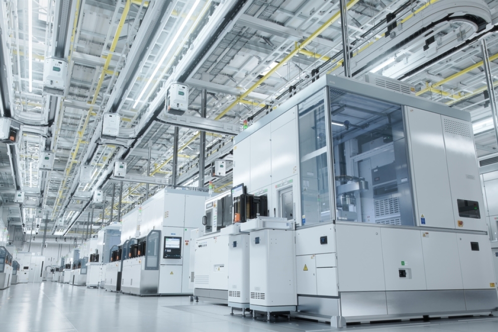
The global semiconductor manufacturing industry is in the throes of change. The last several years have welcomed a new set of challenges that have impacted the industry and propelled it towards innovation. Major trends and requirements are coming to the forefront that will define the future of the semiconductor manufacturing industry, including ensuring supply chain resiliency; the rise of generative AI; fast scalability; meeting OEM’s growing needs across a multitude of markets; navigating geo-political tensions; and developing a diverse workforce. Traditional semiconductor manufacturing processes have inherently weak links and limitations in the ability to manufacture next generation chips which are produced in clean rooms containing a range of equipment used to manufacture CPUs and other advanced semiconductors.
The manufacturing equipment used can include more than 50 different units ranging from epitaxial reactors and chemical vapour deposition systems to photolithography equipment. It is often processes that include ultra-high vacuum (UHV) that dictate the success or failure of product quality and yield in the quest for scalability of advance semiconductor chips.
SLO Cable*
The semiconductor industry continues to grow at a rapid pace with Moore’s law – double the performance, halve the cost - looming above like a long shadow. Amid today’s technological advances what has changed, however, is the influence of several global trends including the rise of Artificial Intelligence (AI), electric vehicles and autonomous driving. In the past, semiconductor growth was attributed to personal computer and mobile innovation but today semiconductor influence is seen in virtually every industry in the modern global economy with even more anticipated breakthroughs to continue as 5G wireless technology broadens demand over the next decade.
An average electrical vehicle, for example, contains 1000-3500 semiconductors used for parts such as MCUs and analog for electric power steering to boost fuel efficiency.1 Given the advancement of automotive intelligence, rapidly changing communication trends and electrification in general, the demand for semiconductors in a multitude of markets will continue to be steady and long-term.
Even as traditional uses for semiconductors continue to exist in high demand, the proliferation of key trends such as hyperscale cloud computing, Internet of Things (IOT) and AI have piled on to the growth trend. Thanks to the increasing need for higher computing power, data processing capabilities, complex language models, and big data analytics in data centers, this technology has very quickly evolved out of its prototype phase and expanded beyond the data center, reaching personal devices driving demand for AI powered chips. McKinsey estimates that the global market for semiconductors is projected to reach $1 trillion by the end of the decade.2 What all of this means is that the production of semiconductors, often seen as the brain of digitization, will remain one of the most valued and traded goods in the world.
Background Empty Chamber*
In addition, increasing demand from a wider variety of sectors, such as automotive and defense, is pushing semiconductor manufacturers to produce smaller, faster and smarter chips at scale. Moore’s law has had the industry increasing transistor densities roughly two times every two years3, which requires manufacturing to continually refine all of its processes. Today, Taiwan Semiconductor Manufacturing Co. (TSMC) transistors are down to just over two nanometers – the smallest in the world with Intel’s transistor density soon to be on par4. The pursuit of these more advanced and powerful chips has led to increasing process complexity because wafer manufacturing is a cycle of defining features with lithography and building them up with deposition, etch, and other process steps to meet key requirements. With ever-shrinking chip features comes mutually with the need for more stringent outcomes, necessitating new equipment with highly controlled environments to minimize contamination of sensitive machine components.
Manufacturing a microchip is no small feat. To make any chip, numerous processes play a role and precision is key.5 As chipmakers push towards smaller nodes, stringent control of molecular contamination becomes critical. Fabs face many hurdles to trust that their metrology equipment is giving them an accurate read of what occurs on the wafers they are processing. For semiconductor processing and fabrication equipment designers and manufacturers, control of airborne particle concentration by introducing vacuum environments is becoming equally crucial.
Extreme ultraviolet (EUV) lithography is seen as one of the biggest breakthroughs for advanced semiconductor manufacturing as the central process for high-volume semiconductor manufacturing. Particle interference, refraction and other physical or chemical defects that occur during this process can massively increase manufacturing costs and significantly increase yield losses. As such, the key challenges in EUV lithography, particularly in semiconductor manufacturing cleanrooms,
stem from the need to control molecular contamination.
Conventional ePTFE Cable*
How does the industry keep up with the increasing challenges?
The industry is approaching the problem from several angles. One key approach involves manufacturers turning to advanced materials and techniques to limit outgassing and maintain a pristine vacuum environment, ensuring that lithography systems can operate with the high precision required for producing next-generation chips. Outgassing occurs when materials, such as cables or other system components, release volatile compounds into the vacuum environment, which can lead to contamination. Additionally, the complexities involved in EUV lithography extend beyond contamination control. The sheer intricacy of the equipment, high costs, and the necessity for a well-trained workforce further complicate its implementation in semiconductor production lines. As a result, cleanroom environments must now be more sophisticated and rigorously maintained to support these operations.
In response to this challenge, Junkosha has developed the cleanest cable assemblies in the semiconductor manufacturing industry to date. Using proprietary manufacturing steps, Junkosha Super Low Outgassing (SLO) cables have the lowest outgassing and particulation levels available on the market, enabling semiconductor manufacturers to maintain an extremely clean environment within their systems. In addition, Junkosha’s cables combine a high level of mechanical flexibility with the ability to integrate multiple cables making it ideal for vacuum chamber environments with moving parts such as linear stages integrated with motors and encoders.
Semiconductor manufacturing is dependent on vacuum technology because it plays an integral part in the efficiency of processes and yield, particularly when producing advanced chips.
Ultra-high vacuum in a processing chamber is generally achieved using a turbomolecular pump located at the processing tool followed downstream by a dry vacuum pump. These sensitive process chambers demand high performing materials that also relates to cabling that are utilized for data and power transmission.
In all vacuum (and non-vacuum) processing equipment, residual gases may originate in the process chamber and even from the contaminated silicon substrates. In the graphs below, we see the results of the RGA testi conducted over 240 minutes on both the SLO cable and a conventional ePTFE cable.
Semiconductor manufacturing requires precision at a swift pace. Because velocity and precision are generally at odds - you move fast, you break things or at a minimum, make unusable product- achieving increased throughput and higher wafer-per-hour speeds places the highest demand on all mechanical components, including cables. By deploying an SLO cable, manufacturers can drastically cut down on the outgassing molecules that latch on to sensitive components such as mirrors and compromise image quality, which directly correlates with the quality of the chip circuitry.
Moreover, SLO cables enable manufacturers to reach the required vacuum levels much faster. This provides an ultra-low pressure environment utilizing vacuum pumps to create advanced chips. Cables and other polymer-based products which do not emit outgas are essential to the success of overall system output.
The graph on the next page breaks down how vacuum levels shift over time across three key factors. The blue line represents the background, while the red line shows our conventional cable which fails to hit the 10^-5 Pa vacuum pressure mark even after 480 minutes. In contrast, the yellow line tracks the SLO cable, reaching that same pressure in just half the time—240 minutes. As a result, there is a substantial reduction in time for customers, driving more efficient operations.
The challenges faced in boosting production
Optimizing process flows has the same level of focus for fabrication equipment designers and manufacturers as it has for fabs. As fabs boost production of silicon chips they simultaneously churn out more liquids, slurries, and gases around the facility placing more pressure on both process and material-handling equipment. This challenge intensifies as line diameters and wafer thicknesses decrease, pushing equipment to meet increasingly stringent requirements. Wet chemical processes used in etching, cleaning, and other stages in chip manufacturing rely on carefully controlled transport of chemicals.
These liquids must be handled in properly sealed containers to prevent leakage of gases or fluids that could compromise safety or purity of the product. Beyond resistance of aggressive chemicals, the materials used must also not contribute organic or trace metallic contamination which could otherwise degrade the effectiveness of the cleaning or stripping fluids.
To address this challenge, manufacturers must use the right equipment to prevent deterioration and gas permeation. PFA stands out as one of the very few materials that is inert, stable, and impermeable enough to handle the aggressive chemicals used in fabs and to keep ultrapure chemicals – including water—free from particles and leachates. Currently, Junkosha High Barrier PFA Tubing is the most durable tubing solution available for piping in wet processes in semiconductor manufacturing. Developed with two heat fusion bonded layers, it has an excellent barrier against strong acids, alkalis and organic solvents, resulting in a reduction in the number of replacements needed.
The inner layer, made from high purity PFA, offers chemical resistance, heat durability and adhesion resistance. The outer layer is made from fluoropolymers with excellent barrier properties against acids (for example hydrochloric acid and nitric acid) from the inside and water vapor from the outside.
Furthermore, the tubing maintains transparency over a long period of time, which is an indicator of lack of tube deterioration. For fabs seeking to reduce downtime, the High Barrier PFA Tubing is the ideal solution due to its unique ability to manage the flow of highly toxic and corrosive materials, helping to reduce maintenance and corrosion of surrounding metal parts.
Change in Pressure vs Time@ SLO Flat Cable*
Safeguarding production output
All manufacturing in the world is built upon stacking multiple processes and systems with various tolerances and variation ranges to get a consistent product. Nowhere is this more evident than in semiconductor manufacturing due to being the single most complicated manufacturing process with the lowest tolerance for error in the world. The global semiconductor supply chain is a web of interdependent, critical links that would take trillions of dollars and at least a decade to fully reconstruct. While TSMC in Taiwan and ASML in the Netherlands are the typical examples of dependencies, there are many more similar representations within the semiconductor supply chain ranging from equipment to chip design. These supply chain dependencies call for businesses to understand the semiconductor industry supply chain’s vulnerability to safeguard production output.
This has brought to the forefront supply chain specialists who possess expertise in the processes surrounding chip production that can make or break the successful fulfilment of orders. Their focus is on strategies that can help the industry curb the bottlenecks for advanced semiconductor manufacturing as demand continues to outstrip supply. For example, delivering quality products is a collective requirement for the entire supply chain.
Given the high R&D investment costs and large capital expenditures, subpar products would have severe ramifications. Even if the physical damage to the fab is avoided, inconsistencies in materials means that equipment breaks down faster and critical chemicals such as photoresist can cause significant variations in circuit lines, potentially grinding fabs to a halt. Similarly, any particulates or molecular contamination caused by outgassing from machine cabling when the cable is bent or moving within the vacuum can condense on sensitive components like electronics, lenses and mirrors or even on the wafer itself, and therefore would have severe consequences.
Consistent manufacturing and stringent quality control measures at every step of the process ensure that Junkosha’s products are trusted for precision and performance. Junkosha Super Low Outgassing Cable portfolio uses a highly controlled end-to-end manufacturing process, starting from our in-house material development of PTFE composite films. After careful material selection, Junkosha conducts a series of stringent cleaning, outgassing and particle reduction steps throughout each part of the complex production process, including planning and design, cable manufacturing, assembly, packaging and RGA evaluation. Through these highly controlled production steps, Junkosha optimises the delivery of high quality cable products with extremely low outgassing and low particulation characteristics. By incorporating these benefits with a long and durable cable life, semiconductor manufacturers achieve a reduction in equipment downtime and a significantly lower number of maintenance interventions.
Conclusion
As semiconductor manufacturers race to meet the demands of new and emerging markets, they are confronted with a complex web of challenges – from maintaining clean room integrity to supply chain complexities across various process technologies.
The need to reduce outgassing and eliminate contaminants is more important than ever as the industry expands into areas like autonomous driving, AI, IoT, next generation mobile electronics and beyond. At the center of these changes is a dependency on vacuum environments that either make or break the quality and scalability of modern chip production. In this evolving landscape, success will depend not just on the technological advances but also on securing long term resiliency of the supply chain with top quality equipment. The future of semiconductors is being shaped in real time and those that are ready to confront the current weak links in manufacturing processes will be the ones leading the charge.


