EV Group to showcase temporary wafer bonding for HBM & 3D DRAM in Korea
EV Group (EVG), a provider of innovative process solutions and expertise serving leading-edge and future semiconductor designs and chip integration schemes, today announced that it is highlighting its industry-leading IR LayerRelease™ temporary bonding and debonding (TB/DB) solution, as well other wafer bonding and lithography technologies, at the SEMICON Korea 2025 expo in Seoul, Korea on February 19-21.
As the market and technology leader in wafer bonding, EVG provides the most complete portfolio of wafer bonding solutions, including TB/DB, which are driving the development and production of high-bandwidth memory (HBM) and 3D stacked DRAM devices that are fueling artificial intelligence (AI) accelerators and other high-performance computing (HPC) applications. AI, along with advanced packaging and sustainable semiconductor manufacturing, is a key focus area for SEMICON Korea, one of the world’s preeminent semiconductor technology expositions showcasing key trends that are shaping the future.
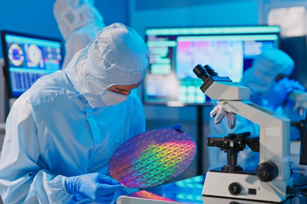
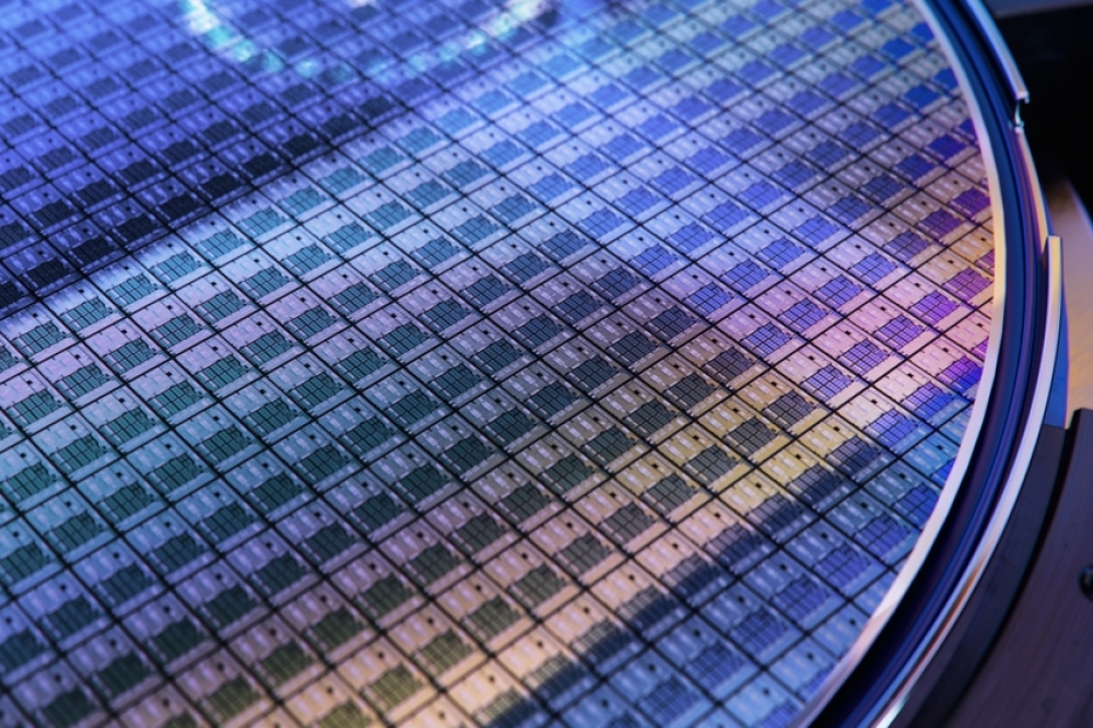
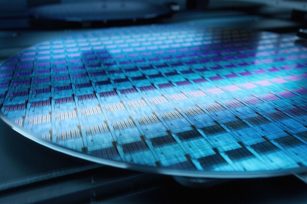
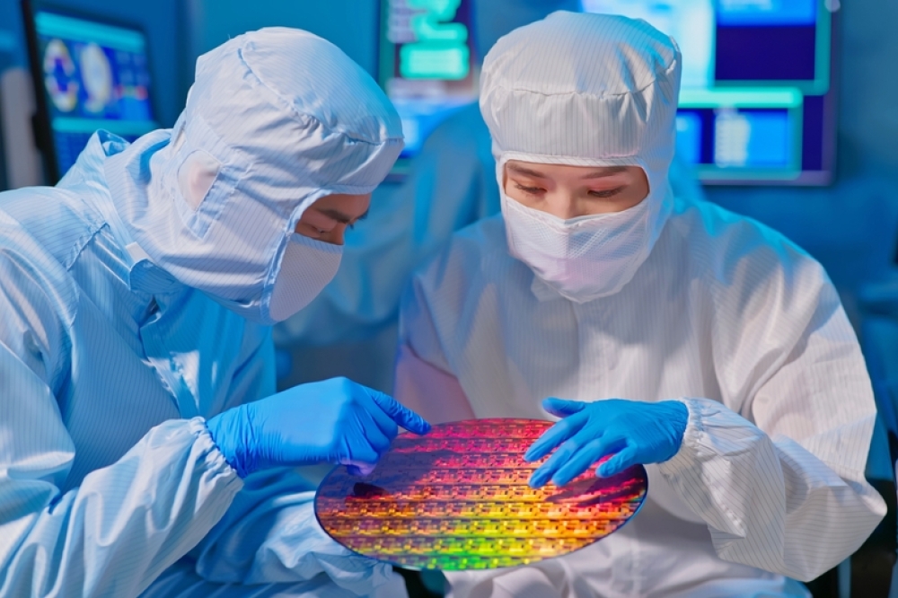
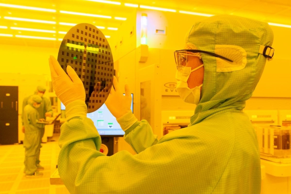
EVG IR LayerRelease™ process development and verification at the leading-edge Heterogeneous Integration Competence Center™ (HICC), located at the company’s global headquarters in Austria. Source: EV Group.
According to Dr. Thorsten Matthias, regional sales director Asia/Pacific for EV Group, “Accelerating the development and volume ramp of next-generation HBM and 3D stacked DRAM is a top priority for the Korean chip industry, fueling the need for advances in temporary bonding and debonding technology. EVG’s IR LayerRelease technology is revolutionizing the market, enabling thinner dies for higher HBM stacks through laser debonding, thereby eliminating the need for mechanical debonding. IR LayerRelease serves as a drop-in replacement for mechanical debonding, supporting silicon carriers in both current and future generations of stacked memory. Additionally, its front-end compatibility allows it to combine with fusion and hybrid bonded process flows, making it ideal for extremely thin wafers and film processing, essential for next-generation memory and logic.”
Temporary Wafer Bonding/Debonding Essential for Advanced Memory
HBM and 3D DRAM have emerged as promising semiconductor technologies to support the growing demand for AI training applications due to their ability to deliver high bandwidth, low latency and low power consumption in a small footprint. Temporary bonding and debonding are crucial process steps for chip stacking, which is mandatory for manufacturing these advanced memory devices. Legacy debonding solutions, such as mechanical debonding, do not have sufficient precision needed for ultra-thin wafers featuring highly complex geometries such as future HBM designs. EVG’s IR LayerRelease solution provides clear advantages in terms of precision, higher yield, lower cost of ownership and environmental impact, as well as future proofing, for memory and other device manufacturers in Korea and beyond. IR LayerRelease replaces mechanical debonding, and complements EVG’s debonding technology portfolio alongside the company’s slide off and UV laser debonding solutions based on the EVG®850 platform.
IR LayerRelease Details
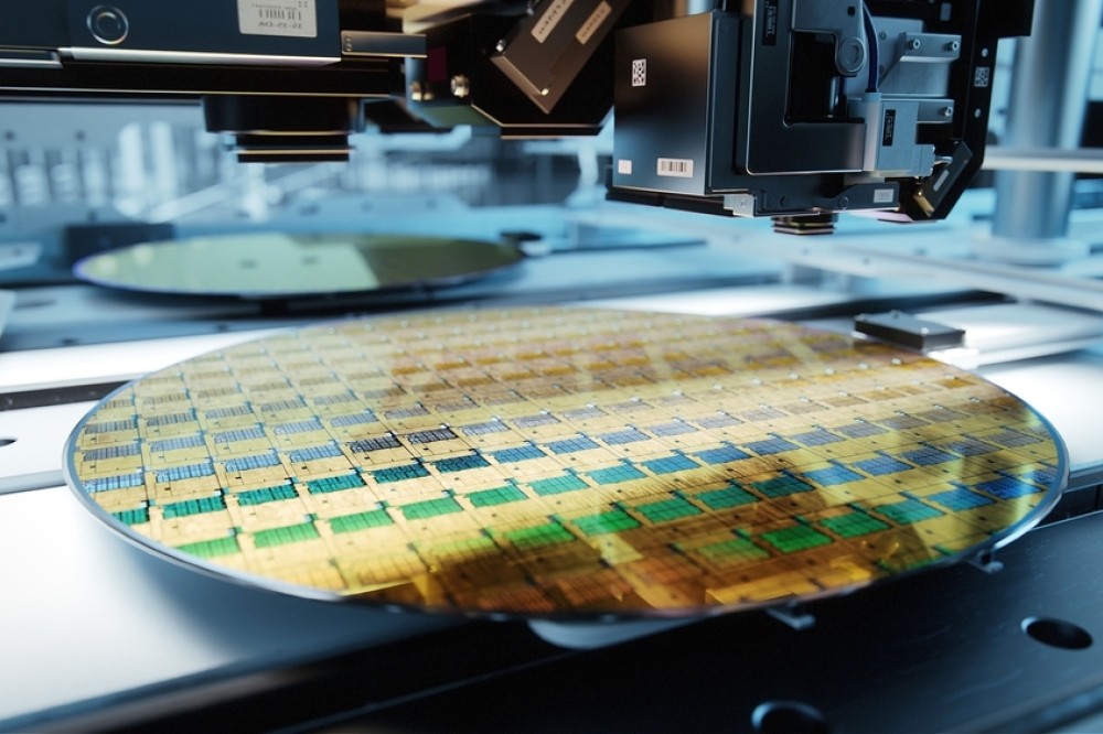
EVG's IR LayerRelease technology is a fully front-end-compatible layer release technology that features an infrared (IR) laser that can pass through silicon, which is transparent to the IR laser wavelength. Coupled with the use of specially formulated inorganic layers, this technology enables laser-initiated release of any ultra-thin film or layer from silicon carriers with nanometer precision and the highest debonding throughput in the industry. As a result, IR LayerRelease eliminates glass substrates for advanced packaging and enables completely novel process flows for 3D-IC and 3D sequential integration applications – enabling hybrid and fusion bonding even of ultra-thin layers on silicon carriers. IR LayerRelease utilizes inorganic solvents for cleaning after IR exposure instead of organic solvents, minimizing the ecological and chemical footprint in the fab. It can be integrated in the EVG®880 equipment platform, which is a fully automated high-volume-manufacturing platform.
EVG at SEMICON Korea
SEMICON Korea attendees interested in learning more about EVG and its innovative process solutions that are enabling advances in AI, HPC, advanced packaging, and sustainable semiconductor manufacturing, are invited to visit EVG at Booth C740 (3rd Floor, Hall C) on February 19-21 at the COEX in Seoul, Korea.