UB researchers mix silicon with 2D materials for new semiconductor tech
The work, from researchers in the UB Center for Advanced Semiconductor Technologies, could lead to energy-efficient microelectronics.
A University at Buffalo-led study, published in the Jan. 6 issue of the American Chemical Society (ACS) journal ACS Nano, explores how mixing two-dimensional materials with silicon might achieve this goal. The article suggests a better way to inject and transport electric charges – an advancement that showcases the significant potential of 2D materials in advancing future semiconductor technologies.
“Our work investigates how emerging 2D materials can be integrated with existing silicon technology to enhance functionality and improve performance, paving the way for energy-efficient nanoelectronics,” said the study’s lead author Huamin Li, PhD, associate professor in the Department of Electrical Engineering. “More complex devices, like three-terminal transistors, can benefit from our discovery, achieving enhanced functionality and performance.”
Fei Yao, PhD, assistant professor in the Department of Materials Design and Innovation, is the study’s co-lead author.
“As scientists, we want to make the components smaller so that they can do more work in less space,” she said. “This will allow us to create advanced technology that is more powerful and compact.”
Li and Yao collaborated with co-author Vasili Perebeinos, PhD, professor in the Department of Electrical Engineering. All three are members of UB’s Center for Advanced Semiconductor Technologies, an interdisciplinary research center that develops cutting-edge microelectronics solutions while training the next generation of leaders for the semiconductor industry.
Additional study co-authors, many of whom are experts in 2D materials, physics and nanoelectronics, work in China, Korea, Austria and Italy.
“This collaboration highlights UB’s leadership in cutting-edge semiconductor research and its ability to foster impactful international and interdisciplinary partnerships,” Yao said.
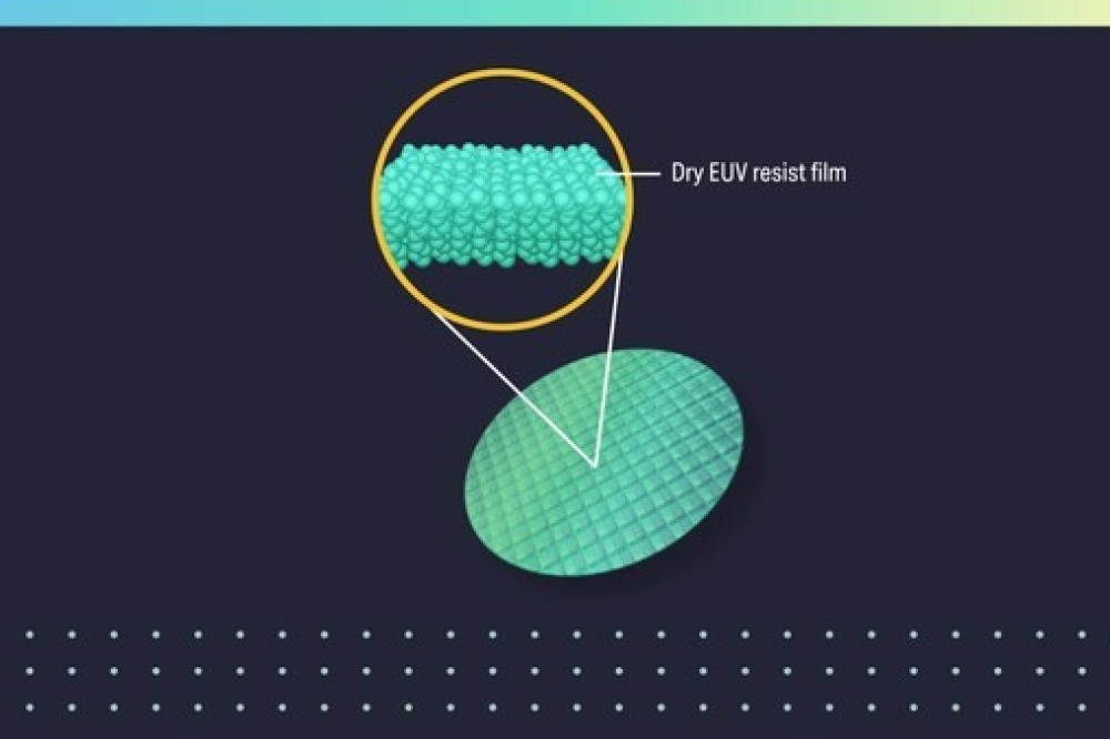
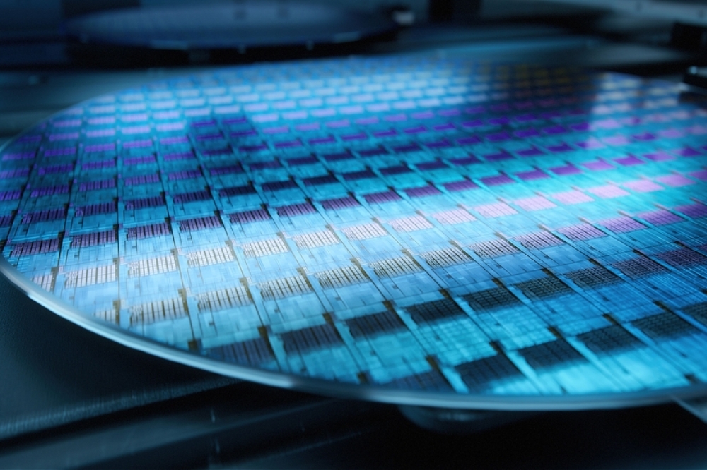
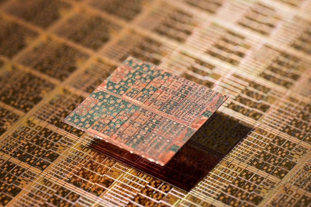
In the study, the team demonstrated that using thin 2D materials, like the semiconductor molybdenum disulfide (MoS2), in combination with silicon, can create highly efficient electronic devices with excellent control over how an electrical charge is injected and transported. The presence of the 2D material between the metal and silicon – despite the MoS2 being less than one nanometer thick – can change how current electrical charge flows.
The 2D material mainly affects charge injection or how the charge enters the material, but doesn’t really affect charge collection, or how the charge exits the material.
“The 2D material mainly affects charge injection or how the charge enters the material, but doesn’t really affect charge collection, or how the charge exits the material,” Li said. “This happens regardless of the specific properties of the 2D material. So, whether you use semiconducting MoS2, semi-metal graphene, or insulator h-BN [hexagonal boron nitride], they can play different roles in the charge injection, but all behave similarly when it comes to the charge collection. Essentially, the 2D material in this special condition acts almost like it’s invisible or has zero resistance for collecting charge.”
While integrating 2D materials with silicon is a promising path for next-generation electronics, Li said, significant challenges remain, particularly in understanding and engineering charge transport where the 2D material meets the 3D material.
“Our study provides critical insights into the energy band structure and charge transport mechanisms at the 2D/3D interface, especially when 2D materials are scaled down to monolayers,” he said. “Over time, this research could inspire the development of new 2D materials and device concepts, ultimately leading to more efficient and powerful electronic devices for everyday use.”
The work was mainly supported by a $608,000 grant from the National Science Foundation (NSF) in December 2019. Additional support was provided by the UB’s Center for Advanced Semiconductor Technologies.