Laser Photonics propels R&D efforts in wafer marking
Laser Photonics and its recently acquired subsidiary, Control Micro Systems, Inc. (CMS Laser), today announced the expansion of theiris expanding its Laser Wafer Marking technology research and development program.
“By integrating CMS Laser’s expertise with our advanced R&D initiatives, we are committed to providing chip manufacturers with the most sophisticated laser wafer processing systems”
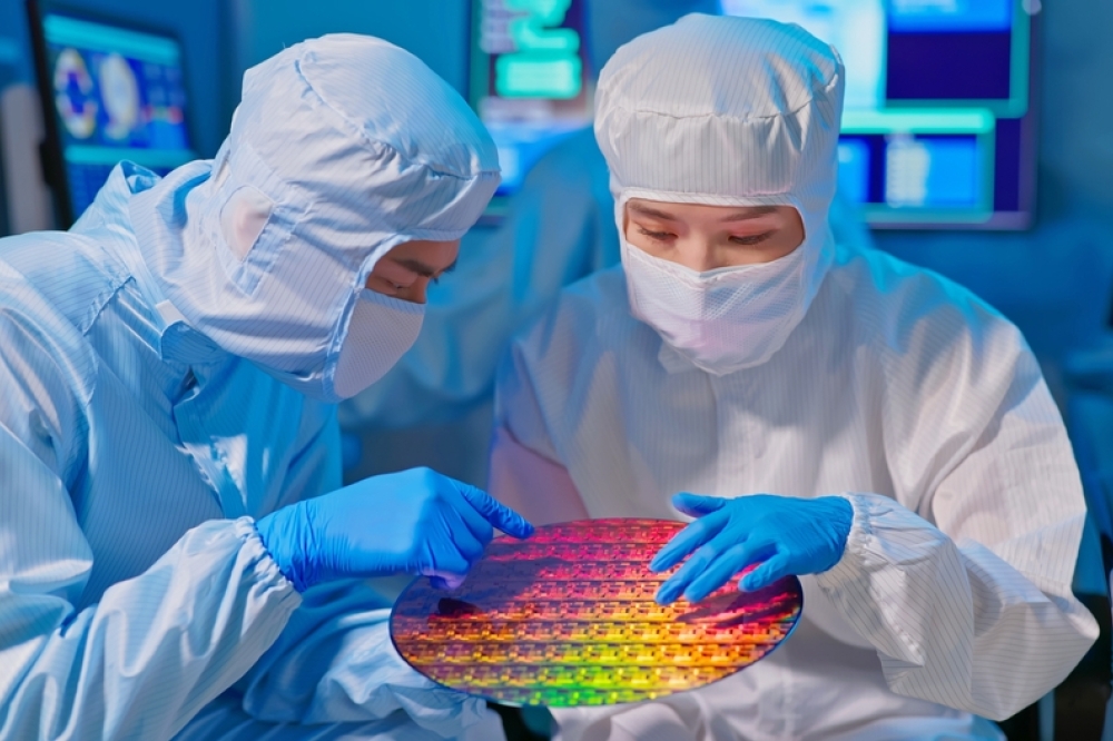
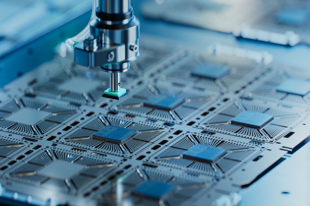
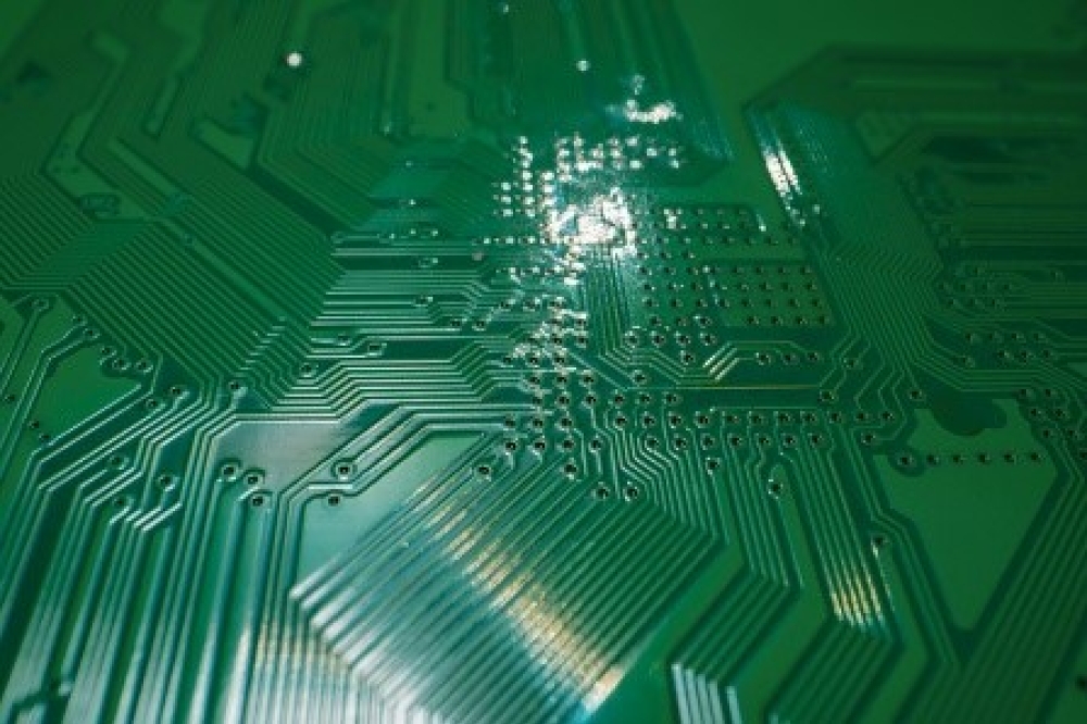
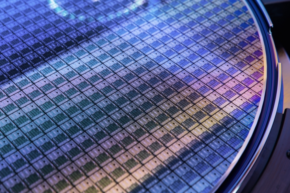
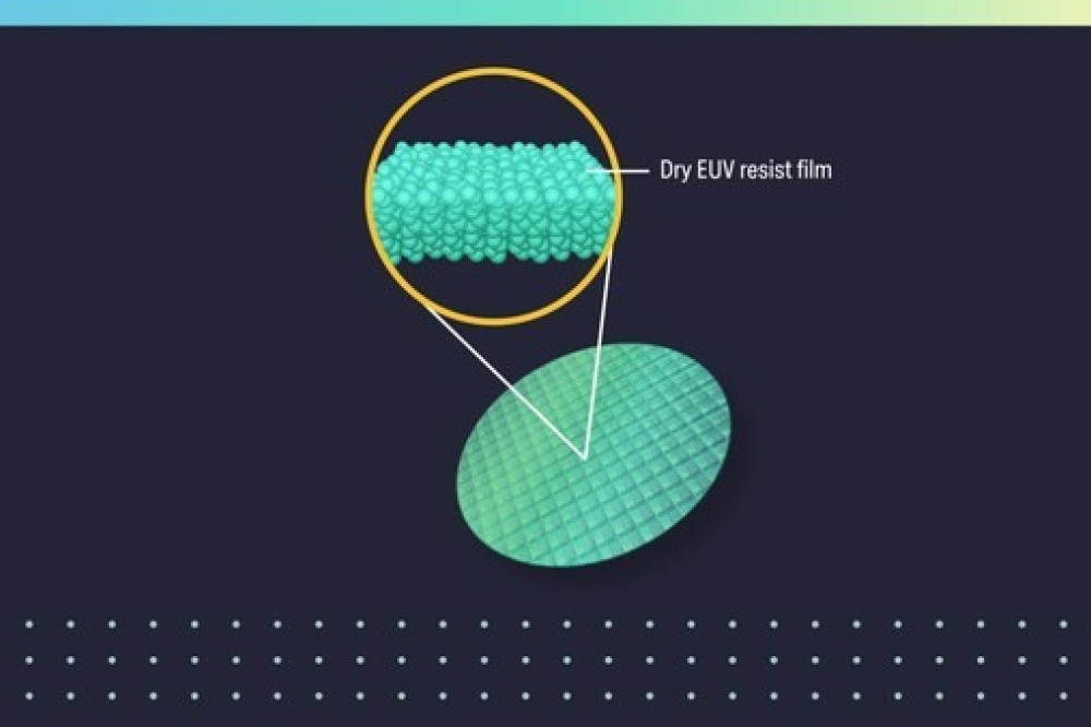
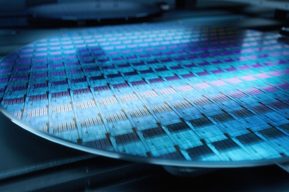
High-precision Laser Wafer Marking technologies are designed for engraving serial numbers and other critical information on silicon and compounds used in the semiconductor industry.
“By integrating CMS Laser’s expertise with our advanced R&D initiatives, we are committed to providing chip manufacturers with the most sophisticated laser wafer processing systems,” said John Armstrong, Executive Vice President of LPC. “We are ready to support fabs in the United States and abroad amidst the ever-growing demand for chips and the regulatory stimulation of the sector.”
CMS Laser’s cutting-edge laser marking technology is designed with custom configurations for each client, including the laser type, product transport and handling, machine vision, and fume extraction. Engineers can tailor the process to accommodate virtually all specific needs, including integrating seamlessly with existing databases, connecting to sophisticated Surface Mount Technology (SMT) lines, incorporating external stackers and destackers, adopting various flipping configurations, or robotics integration.
CMS Laser prides itself on working with the end user to create a solution that integrates into their manufacturing environment and accepts engineering challenges that other laser system companies turn down.
Developed to meet the most demanding requirements, CMS Laser’s laser marking systems deliver unrivaled performance, making them an indispensable asset in advanced wafer processing. Chip manufacturers can rely on these innovative systems to enhance production, with precision, speed, and adaptability providing a remarkable competitive edge, ensuring accurate, uniform results in every batch.
Leveraging CMS Laser’s specialized expertise, LPC is directing resources into R&D for laser wafer marking, aligning with its broad diversification strategy. This initiative is designed to boost shareholder value and strengthen resilience in dynamic markets. For more information about Laser Wafer Marking Systems or LPC’s lines of cleaning, cutting, welding, marking, or engraving laser systems, visit https://www.laserphotonics.com.