Applied Materials and Arizona State University celebrate Opening of ‘Materials-to-Fab’ Center
A ribbon-cutting event was held at the Center as semiconductor industry leaders from around the globe gathered in nearby Phoenix for the SEMICON West conference.
Applied Materials executives, including Dr. Prabu Raja, President of the Semiconductor Products Group, and ASU President Michael Crow were joined at the ribbon-cutting by Arizona Governor Katie Hobbs and other government and city leaders to highlight the benefits that the MTF Center will bring to Arizona and the entire semiconductor industry.
“The work of advancing discovery and with it, the American semiconductor manufacturing industry, is of vital importance to the nation from both an economic competitiveness and a national security perspective,” said Arizona State University President Michael Crow. “The alliance between a global industry leader like Applied Materials and a leading research university like ASU and the work that will be done in the Materials-to-Fab Center will lead to breakthroughs and acceleration that enable chip manufacturers in the United States to lead the world in developing the technology that we need today and in the future.”
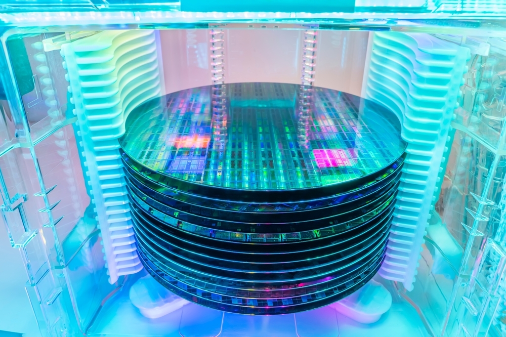
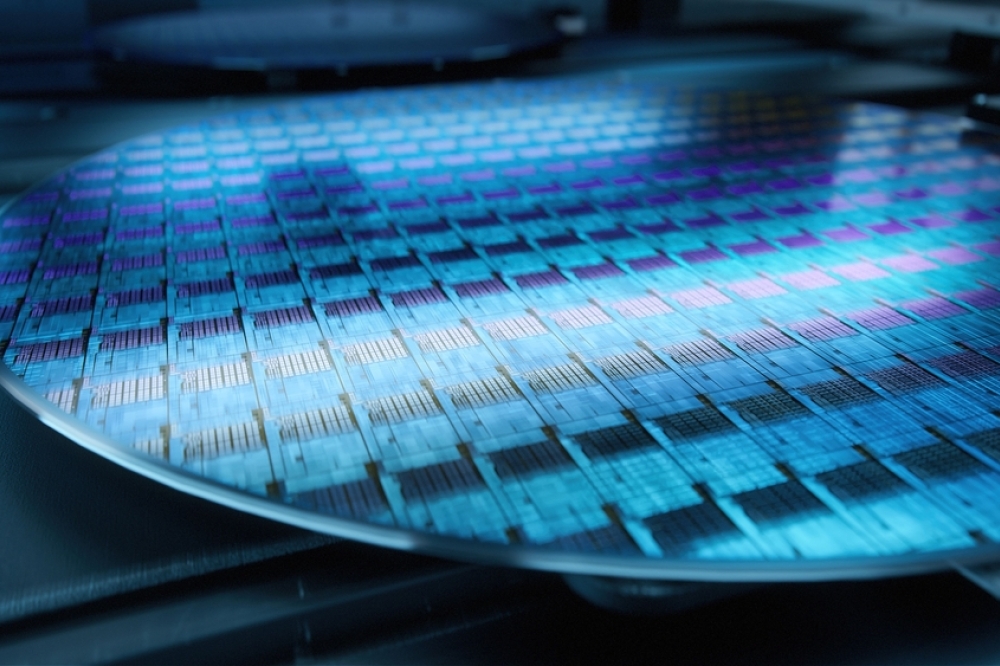
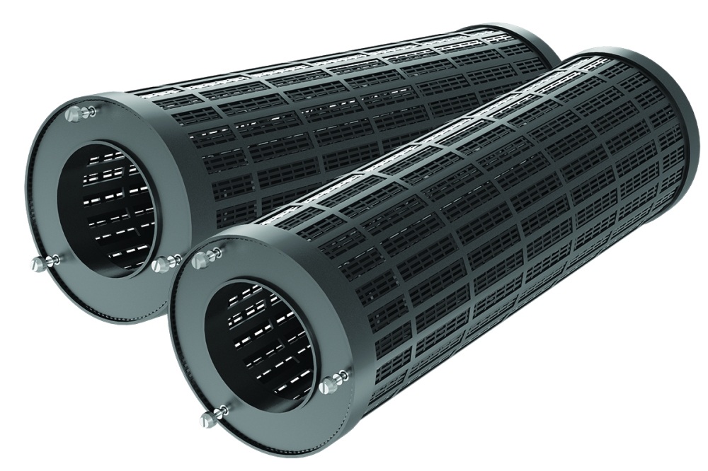
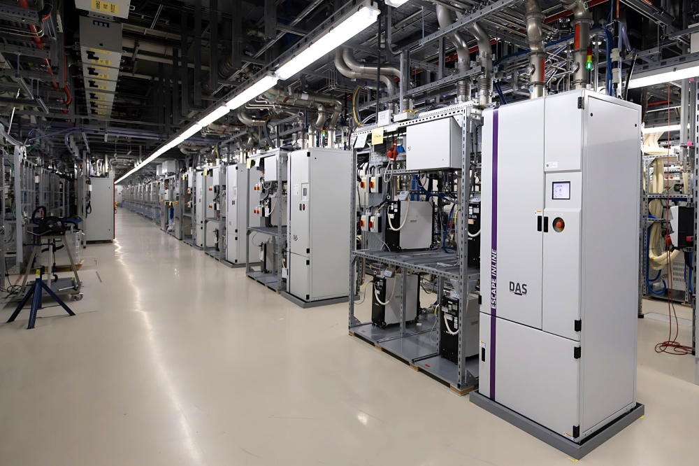
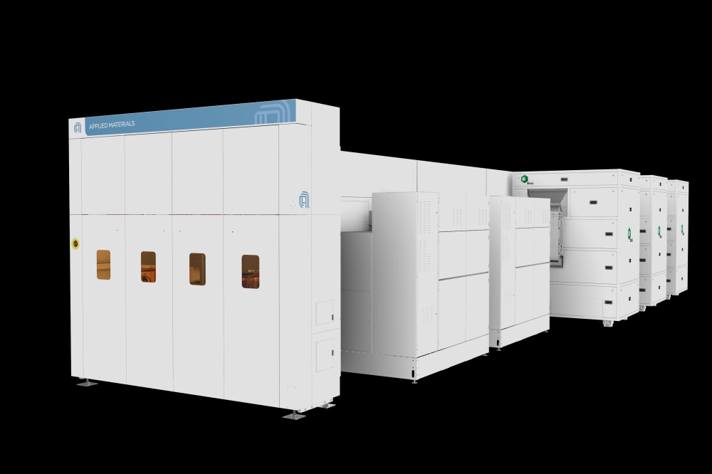
The Materials-to-Fab Center is designed to accelerate the transfer of innovations from ideation to fab prototype by bringing Applied Materials’ state-of-the-art semiconductor manufacturing equipment into a collaborative environment where the university, industry partners, startups, government entities and other academic institutions can work together.
Dr. Prabu Raja, President of the Semiconductor Products Group at Applied Materials, said, “Universities are the foundation of America’s semiconductor innovation pipeline, and we look forward to bringing together ASU’s world-class engineering teams with Applied Materials technologists and ecosystem partners at the Materials-to-Fab Center. These collaborations will focus on accelerating development of new chip technologies that are crucial to U.S. leadership in AI, high-performance computing and other megatrends shaping the future.”
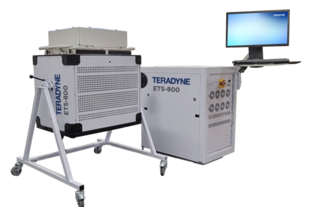
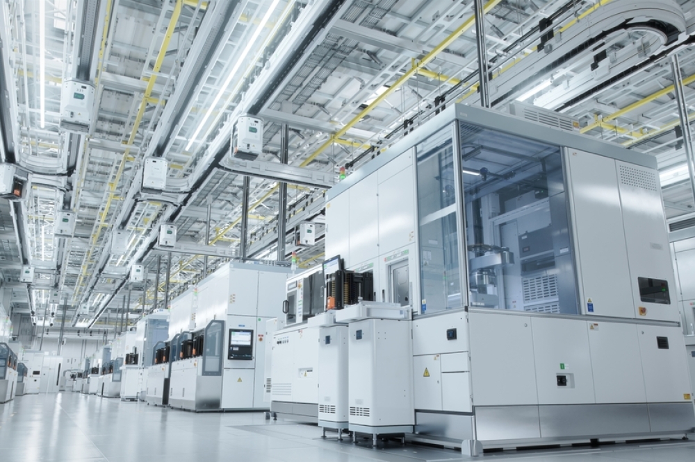
Applied Materials is the largest U.S. producer of semiconductor manufacturing equipment. Its tools are used to produce virtually every new chip in the world. The company’s major U.S. production facilities are located in Texas, Massachusetts, Montana, and a new site under development in Chandler, Arizona. The centerpiece of Applied’s research and development initiatives is the EPIC Center in Silicon Valley. On track to open in 2026, the EPIC Center will be the world’s largest and most advanced facility for collaborative semiconductor process technology and manufacturing equipment R&D.
Arizona State University has emerged as one of the nation’s leading universities in helping to shape the future of American microelectronics. As the recipient of several large investments from state, federal and private sector stakeholders, ASU conducts work across the entire microelectronics ecosystem – from front-end innovation to advanced packaging and large-scale manufacturing. With the largest engineering school in the country – approximately 33,000 students – ASU is also a driving force behind workforce and talent development.
“The Materials-to-Fab Center is a marriage made for Arizona and something that will benefit the entire region,” said Arizona Governor Katie Hobbs. “Applied Materials is an industry leader that already has a presence in the state with many of its customers invested in doing work within the ecosystem that is growing here and Arizona State University is a powerful force behind all the work being done, producing both the people who will lead this industry into the future and the ideas that will shape its progress. I am grateful to the Arizona Commerce Authority for helping this all come together and very excited to see this contribution to our economy coming to realization.”
The MTF Center builds on Applied Materials’ existing presence at ASU’s MacroTechnology Works facility as well as the research already being funded by the company involving ASU faculty and students. The Center is also already making contributions to ASU projects awarded through the CHIPS and Science Act for the Southwest Advanced Prototyping (SWAP) Hub, which is advancing rapid translation of technologies for national defense and the SHIELD USA project, which is focused on advanced packaging technologies.
“The launch of the Materials-To-Fab Center ushers in a new era for U.S. semiconductor innovation, providing a one-of-a-kind platform where innovators can test, refine, and accelerate new processes and technologies,” said Sandra Watson, President and CEO of the Arizona Commerce Authority. “This pioneering collaboration between Applied Materials and ASU strengthens Arizona’s position as a national leader in semiconductor R&D, and we’re proud to support this transformative initiative.”
“The physical space that this delivers and the tools provided by Applied Materials through this alliance are a very important part of the Materials-to-Fab Center,” said Sally Morton, Executive Vice President of ASU’s Knowledge Enterprise, which leads research for the university. “But it’s also a place for the experts in this field, ASU faculty and industry leaders, to come together and share ideas. Applied Materials bringing the voice of the customer and ASU adding the curiosity and creativity of its students. We’re very excited about what will happen here.”