Semiconductor inspection equipment set for 7.9% CAGR growth through 2034
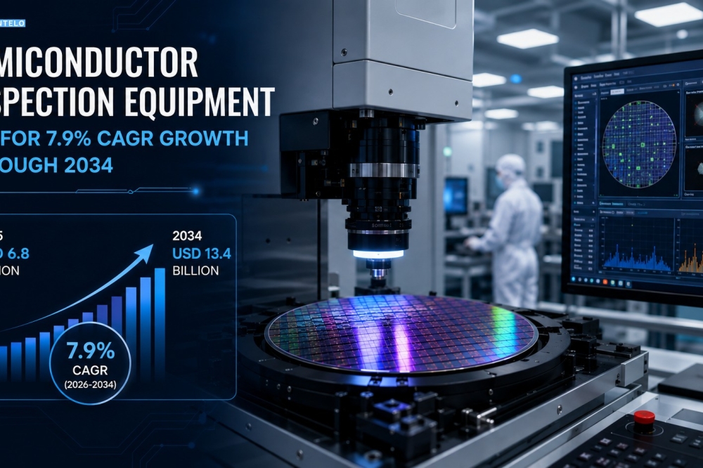
The robust growth rate can be attributed to increased demand for advanced node logic devices along with quick implementation of AI in semiconductor inspection equipment.
It is forecasted that the global semiconductor inspection equipment market will experience a growth rate of 7.9% from 2026 to 2034 and will attain a market value of USD 13.4 billion by 2034. The high growth rate is attributed to the declining process nodes, AI-enabled defect classification, and adoption of advanced packaging techniques.
Why Inspection Equipment Has Become a Critical Component
Current chip production processes leave very little margin for error. With shrinking geometries below the 3nm node, a single defect could cause significant damage to the yield rate of chips produced on that wafer. This is why the development of inspection and metrology equipment has transitioned from an auxiliary process control step to the most critical category of capital equipment in the fabrication facility.
Semiconductor inspection equipment includes the equipment used to inspect for defects, contamination, and pattern anomalies on wafers during their fabrication process – from the inspection of bare-wafer surfaces, patterned layer defects analysis, CMP endpoint detection, and wafer packaging inspection. With the shrinking defect budget of semiconductor manufacturers at the advanced process nodes, the use of this equipment has transitioned from the back-office to the core of the fab investment strategy.
Recent Developments Shaping the Market
Several recent events show how rapidly this market is changing:
Advanced node transitions are driving new categories of defects. The shift to gate-all-around (GAA) nanosheet transistors, now in commercial production at Samsung and ramping at TSMC, has introduced three-dimensional channel structures that traditional brightfield optical tools cannot fully characterize. This has accelerated demand for electron beam inspection systems capable of resolving sub-surface and buried-interface defects.
AI-powered inspection has gone mainstream. Automated defect classification (ADC) systems, once limited to roughly 70–80% accuracy under rule-based logic, are now achieving above 95% accuracy while cutting nuisance alarm rates significantly. Leading equipment makers have folded machine learning directly into their inspection platforms, and AI-enabled systems are commanding a notable price premium over legacy tools a trend that is lifting average selling prices across the market, not just unit volumes.
Advanced packaging is opening a new front-end-to-back-end demand channel. Hybrid bonding, fan-out wafer-level packaging, and 2.5D/3D chip stacking require inspection of bond pads just 1–2 micrometers in pitch, pushing adoption of X-ray CT, scanning acoustic microscopy, and 3D optical profilometry tool categories that sit largely outside the traditional front-end inspection suite.
Government-backed fab construction continues to expand the installed base. Acts like CHIPS and Science Act of USA, European Chips Act, and Japanese Semiconductor Incentives by METI are responsible for triggering a spate of new fab projects not only in the US, Germany, Japan, but worldwide. Every new fab is a new multimillion dollar contract for inspection and metrology equipment starting from litho verification to wafer sort.
Market Outlook 2025–2034
In terms of region, Asia Pacific continues to be the main contributor to demand in the market accounting for nearly half of the total global market value in 2025 due to the presence of highly advanced foundries and memory fabs in Taiwan, South Korea, Japan, and China. North America stands second as a market segment followed by Europe, where its contribution is due to lithography and process control applications owing to fabs located in Germany and Ireland. The regions of Latin America and Middle East & Africa continue to contribute smaller shares but higher growth rates due to the development of electronics manufacturing ecosystems.
Optical inspection technology holds the dominant position in the market owing to its high throughput capacity and cost-effectiveness in various process layers, yet electron beam inspection is expected to be the fastest growing technology segment through 2034 due to the emergence of defects, which can only be detected by e-beam resolution owing to EUV lithography and multi-patterning. On the application side, defect detection remains the largest use case, while metrology covering critical dimension measurement, overlay, and film thickness is growing at a faster clip as 3D device structures demand more volumetric characterization. Looking at technology dimensionality specifically, 3D inspection is the standout growth category, expanding roughly 3 percentage points faster annually than 2D methods as NAND stacks exceed 300 layers and advanced packaging interfaces require full volumetric inspection.
Industry Context: A Capital Equipment Cycle Unlike Prior Ones
To understand why inspection equipment specifically is outgrowing the broader chip market, it helps to look at what is happening one level up, in overall wafer fab equipment (WFE) spending. Industry association SEMI has repeatedly revised its equipment spending forecasts upward through 2026, now projecting worldwide 300mm fab equipment spending to rise 18% to roughly $133 billion in 2026 and a further 14% to about $151 billion in 2027 — the first time the industry has crossed the $150 billion mark. SEMI has attributed this to AI-driven data center and edge compute demand resetting the scale of semiconductor manufacturing investment, alongside continued national self-sufficiency programs.
That broader capex surge matters for inspection equipment specifically because process-control tools are consuming a rising share of every dollar spent on new fab capacity, not a fixed one. KLA Corporation, the market's dominant vendor, closed fiscal 2026 (ended June 30, 2026) with $13.58 billion in total revenue and told investors that its Advanced Packaging process control systems revenue is now expected to grow to approximately $1.1 billion in calendar 2026, up more than 70% year-over-year nearly twice the growth rate of the advanced packaging market itself.
On the company's fiscal Q4 2026 earnings call, CEO Rick Wallace pointed to accelerating investment tied to AI infrastructure, continued strength in leading-edge foundry logic, and increasing process control intensity across memory and advanced packaging as the drivers behind the quarter's record revenue. That single data point inspection revenue growing roughly twice as fast as the underlying packaging market it serves is a useful proxy for the "rising content per wafer" dynamic that underpins the 7.9% CAGR forecast for the broader inspection equipment category.
Regulatory Developments Senior Decision-Makers Should Track
Export policy has become as important to this market's near-term trajectory as technology roadmaps. Three developments stand out:
VEU status expiration reshapes China-based fab operations. VEU authorization for the three firms, which allowed TSMC, Samsung, and SK Hynix to purchase U.S.-controlled semiconductor manufacturing tools and ship them to their Chinese facilities on an individual basis instead of having to receive shipment-by-shipment authorization, expired on December 31, 2025. On January 1, 2026, all three firms have been required to apply individually for their own annual export licenses from the Bureau of Industry and Security (BIS). All three received approval for the current cycle, but the shift from a standing exemption to an annually renewable license gives Washington a lever it can adjust every year — a meaningful planning variable for any inspection equipment OEM serving these accounts.
Congress has been advocating for stronger measures than those adopted by the executive branch. In February 2026, a bipartisan congressional delegation formally requested the Departments of Commerce and State to switch from the current case-by-case policy concerning the export of semiconductor manufacturing equipment to China to a blanket ban since, once in the country, the controls regarding end use are practically impossible to enforce. Furthermore, in January 2026, the Foreign Affairs Committee of the House of Representatives introduced a bill that would give Congress a veto right over AI chip export licenses which now rest with the Department of Commerce. Both bills have yet to pass but indicate that the regulation concerning the export of inspection equipment that can be used in sub-14nm manufacturing is ambiguous.
China's capital spending is proving more resilient to controls than the equipment mix. SEMI data shows China is expected to retain the largest single-country share of global 300mm fab equipment spending even as growth moderates, with 2026 outlays estimated around $39 billion sustained largely by mature-node capacity expansion under central government support, even as the most advanced inspection and lithography tools remain restricted. For OEMs, this bifurcates the China opportunity: robust volume demand for inspection tools qualified for mature nodes (14nm–28nm and above), alongside a structurally capped ceiling on sales of leading-edge e-beam and EUV-related inspection systems.
Adoption Trends Worth Watching
Beyond the headline CAGR, a few adoption patterns are shaping how and where inspection budgets are being spent:
• Process control intensity is rising faster than wafer starts. Rather than inspection equipment demand tracking unit volume growth in chip production, fabs are adding more inspection and metrology steps per wafer at each successive node — a trend KLA and other vendors have specifically called out as a distinct growth driver from unit volume.
• Advanced packaging inspection is shifting budget outside the traditional front-end. With KLA's advanced packaging process control revenue growing roughly 70% year-over-year against overall company growth in the high teens, back-end and mid-end-of-line inspection categories (X-ray CT, scanning acoustic microscopy, 3D optical profilometry) are becoming a distinct budget line for OEMs and fab operators rather than an adjunct to front-end tool sets.
• AI-native purchasing decisions. Machine learning has been heavily integrated into inspection processes, leading fab facilities to focus just as much on the accuracy of the classification process and reducing false positives as on the resolution of optical and electron beam systems.
• License-cycle risk is entering vendor account planning. With annual re-licensing now required for equipment shipments into major Chinese-operated fabs, OEMs serving these accounts are having to build regulatory renewal risk directly into revenue forecasting and inventory planning in a way that wasn't necessary under the prior VEU framework.
Key Growth Factors
• Shrinking process geometries: Sub-3nm and emerging angstrom-era nodes are tightening defect budgets to the point where inspection intensity per wafer is rising sharply, particularly at leading foundries running well over 100 in-line inspection and metrology steps per advanced logic wafer.
• AI and automation: Machine learning-driven defect classification and "virtual inspection" techniques are improving detection accuracy while helping fabs prioritize which wafers need physical inspection, adding both efficiency and revenue-per-tool gains.
• Heterogeneous integration: The move away from monolithic scaling toward chiplets, interposers, and hybrid bonding is creating an entirely new demand pool for back-end and mid-end-of-line inspection tools, evidenced by the outsized growth rates vendors are now reporting in this category specifically.
• Fab build-out due to policy: Both the reshoring efforts and the diversification geopolitically for semiconductor production capacity are keeping up a multi-year pipeline of fab construction, each of which demands an entire set of process control tools — a pipeline SEMI now forecasts will help drive annual 300mm equipment spend beyond $150B beginning in 2027.
• Increase in chips for autos and AI: Electric cars and AI accelerators require very tight defect levels, which increases the need for inspection capability in logic, memory, and power semiconductors.
Challenges on the Horizon
The market's growth is not without friction. Export control policy is now an active, moving variable rather than a settled backdrop: the end of VEU status for Chinese fab operations, congressional pressure for a blanket SME export ban, and BIS's annual license-renewal cycle all introduce a layer of regulatory uncertainty that inspection equipment OEMs did not have to underwrite as heavily even two years ago.
The industry is still vulnerable to the cyclical nature of semiconductor capital spending that has been evident for years, with capital spending in memory especially susceptible to volatile swings dependent on pricing trends for DRAM and NAND. And the expense and engineering complexity of advanced-generation inspection equipment, particularly EUV mask inspection equipment, continues to increase the barriers to entry, with competitive advantage held by few suppliers and with smaller fabs and OSATs relying on financing or service-based business models to gain access to state-of-the-art technology.
Key Insights for Decision-Makers
Collectively, the data suggests that the industry is no longer growing just because there are more chips being made – it is growing because each succeeding generation of chips is requiring more inspection and metrology content than the previous one. For fab operators, this argues for treating process control capacity planning as a multi-year commitment tied to node roadmaps and packaging strategy, not a line item that scales linearly with wafer starts. For equipment OEMs and their investors, the advanced packaging and 3D inspection categories currently offer the clearest evidence of demand outpacing the broader market, while exposure to Chinese fab customers now carries a regulatory renewal risk that warrants explicit scenario planning. And for policymakers and industry observers, the inspection equipment market has become a useful, fast-moving barometer of how national semiconductor strategies, export policy, and the AI infrastructure buildout are intersecting in real time. Precision has stopped being just a manufacturing requirement it has become a genuine point of competitive and strategic differentiation heading into the next decade.
Read A Full Report: https://dataintelo.com/report/semiconductor-inspection-equipment-market
Author Bio -
Ashish Kolte is a Marketing Manager at DataIntelo with expertise in marketing, market intelligence, and business strategy. He combines marketing insights with industry research to analyze market trends, identify growth opportunities, and provide data-driven perspectives on emerging industries and global business developments.
LinkedIn: https://www.linkedin.com/in/ashishkolte/