Expert insights on choosing the right test methods for accurate thin film and semiconductor analysis
Kalle Niiranen, Technical Account Manager at Measurlabs, writes about method selection based on his experience managing analysis projects for dozens of clients working with thin films and advanced semiconductor components. Measurlabs is a laboratory testing provider with specialised services for the semiconductor industry, offering seamless access to all analytical techniques through a single point of contact.
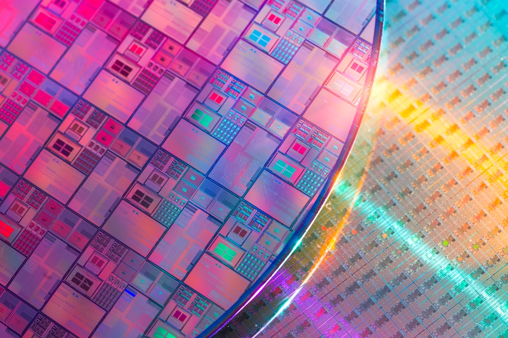
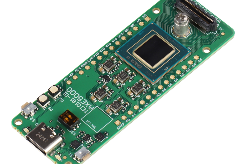
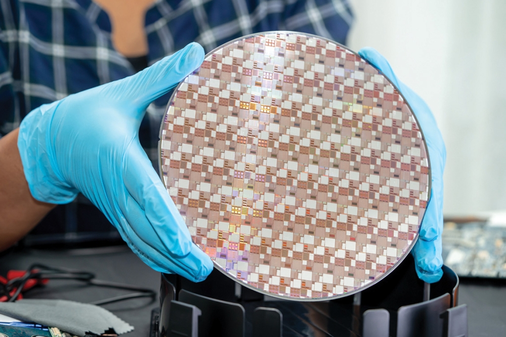
In the semiconductor industry, precision is everything. When devices are scaled down to the nanometer range, the slightest impurity or structural inconsistency can compromise performance or cause the device to fail. Accurate testing is the key to avoiding such situations, and it requires selecting the right analytical method for each task.
Different techniques provide different types of data, and a combination of several methods is often needed to gather all required information. The challenge lies in matching the techniques to the samples and the information needed, whether that is compositional detail, contaminant detection, or structural integrity.
The risks of going for convenience in compositional analysis
Even highly experienced product development engineers often default to familiar or readily available techniques, even when alternative methods could provide more accurate, relevant, or cost-effective results. One situation where we see this often is automatically opting for X-ray photoelectron spectroscopy (XPS) for compositional analysis of thin films. While XPS is an excellent choice for surface-level elemental analysis when quantifying heavier elements, it cannot detect hydrogen or helium. As one example, films deposited using atomic layer deposition (ALD) may be hydrogen-rich, and analyzing them with XPS can lead to deceptively “clean” data that underrepresents hydrogen content by several atomic percentages.
In such cases, a hydrogen-sensitive method like secondary ion mass spectrometry (SIMS) or time-of-flight elastic recoil detection analysis (ToF-ERDA) is needed to obtain a more accurate picture of the film’s composition. Out of these options, SIMS is often chosen simply because it is more well-known. This may introduce a new set of problems, as SIMS requires high-quality reference samples for calibration, and obtaining these for all materials of interest for a suitable matrix is not always straightforward. ToF-ERDA, on the other hand, yields quantitative results for elements from hydrogen to uranium without a need for references.

Picking the right tools for tracking trace contaminants
When analyzing trace-level contaminants on thin film surfaces, the distinctions between methods become even more critical. A common tendency is to opt for a reasonably priced screening method, such as vapor phase decomposition ICP-MS (VPD-ICP-MS). While it is a cost-effective option for routine monitoring and has an excellent, often ppb-level detection limit, it cannot locate the exact spot where the contamination is located on the wafer.
To complement data obtained with VPD-ICP-MS, total reflection X-ray fluorescence (TXRF) can be used to localize the contamination and facilitate a more targeted analysis of its root causes. Due to the higher cost, however, TXRF is typically used sparingly. A typical workflow might involve screening hundreds of wafers for contamination with VPD-ICP-MS and following up with TXRF on a smaller subset of samples.
When measuring trace element concentrations as a function of depth, SIMS is again often the first choice for many. While it does offer an excellent detection limit when references are available, its depth resolution is not always as good as that of medium energy ion scattering (MEIS) spectroscopy, which also has the added advantage of not requiring reference samples.
Depending on the target elements and the required detection limit and depth resolution, Rutherford backscattering spectrometry (RBS) might also be a solid choice. As a general rule, we would recommend ToF-ERDA or SIMS for light elements, MEIS for elements in the mid-range of the periodic table, such as manganese, tin, and gallium, and RBS for the heaviest elements.
Monitoring thin film thickness: why ellipsometry isn’t always enough
Method choice matters even in seemingly routine tasks like measuring thin film thickness. Here, ellipsometry is often used due to its speed and widespread in-house accessibility. However, it can be unreliable for complex multilayer structures or films grown by ALD, where growth-per-cycle values within the film stack may deviate from average results of thicker single-material films. In such situations, variations from the expected layer thickness can lead to inaccurate modelling and misleading thickness data.
X-ray reflectivity (XRR) often provides more accurate results for multi-layered films, especially when the layers have varied densities, which can also be determined with the technique. Additionally, transmission electron microscopy with focused ion beam preparation (FIB-TEM) can be used for visual confirmation of layer thickness in nanoscale films.
The importance of choosing the right testing partner
Availability bias may cause method selection to be guided by the availability of analytical equipment rather than the research question, leading to incomplete or even misleading data being collected. Measurlabs’ service model, built around a wide network of partner laboratories, gets around this issue, as it removes the incentive to recommend a given method just because it is easily available.
Having a scalable testing infrastructure with multiple partners for all major thin film analysis techniques, Measurlabs is well-equipped to manage large-scale projects involving hundreds of wafers or complex multi-technique workflows. Not depending on a single instrument or facility also minimizes the risk of delays caused by equipment downtime or laboratory closures.
In a field where small errors can have large consequences, it is essential to have timely access to a comprehensive range of analysis methods and the expertise to choose the right ones for each purpose. This ensures that results are reliable, costs are kept in check, and incomplete information does not cause delays to product development or quality assurance processes.