Glass in semiconductors: the next inflection in semiconductors
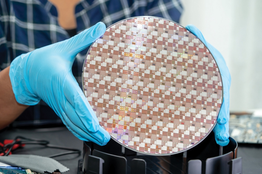
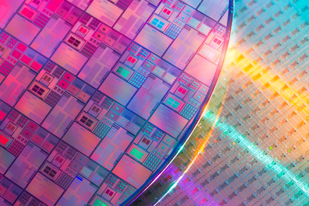
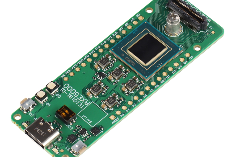
Ultra-flat borosilicate carriers hold silicon wafers during backside thinning, sodium-free sheets form hermetic MEMS caps, and low-coefficient of thermal expansion (CTE) glass is the baseplate for many wafer-level fan-out processes.
Glass is gradually moving from a background consumable to the heart of a package, providing the core substrate, the interposer that links chiplets, and the dielectric that shapes sub-THz signals or steers photons on their way to optical fiber.
IDTechEx has released a brand-new market report, "Glass in Semiconductors 2026-2036: Applications, Emerging Technologies, and Market Insights", providing end-to-end market intelligence for seven distinct glass product segments, with technology deep-dives, benchmarking, supply chain mapping, adoption drivers, risk analysis, and unit and revenue forecasts 2025-2036.
From silent carrier to advanced packaging
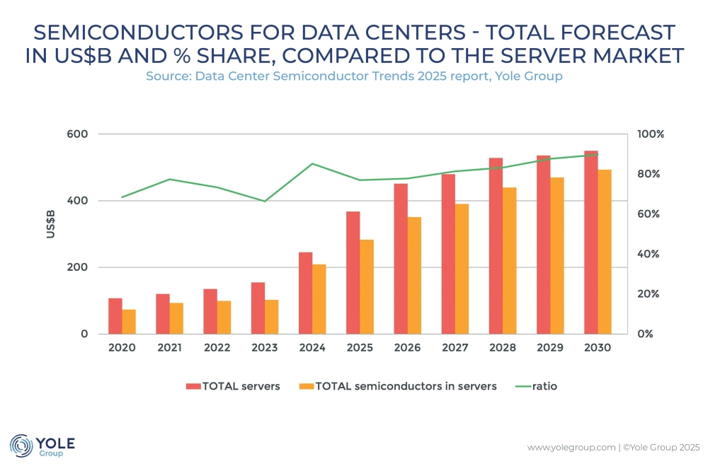
The catalyst in the shift for glass is the escalating bandwidth and power density of AI and high-performance computing devices. A single training accelerator already requires thousands of high-speed I/O bumps and a power-delivery network that handles hundreds of amps with minimal noise. Organic-based laminate, the workhorse of the last twenty years, struggles to maintain the required flatness and via density in response to ever-increasing demand. Silicon interposers offer far finer wiring, but at a price and panel size that limited applications can justify.
Glass slides neatly between these extremes. Its coefficient of thermal expansion can be tailored to match silicon; its loss tangent is an order of magnitude lower than silicon at 40 GHz, and large-panel processing potential from the LCD industry means a single sheet can be half a meter on one side at costs that trend towards high-end organics as yields rise.
The surging demand for AI and high-performance computing is forcing every layer of the packaging stack to carry more current, more I/O, and higher signaling speeds than organic laminates or even first-generation silicon interposers can comfortably support. These pressures have turned glass core substrates and large-panel glass interposers from a niche curiosity into commercialization.
Leading device makers and materials vendors are now openly investigating the technology: Intel has demonstrated glass-based test vehicles on its Arizona path-finding line, Samsung Electronics is exploring glass cores as a potential option alongside its I-Cube and H-Cube packages, substrate major SKC has installed a pilot drill-and-fill line for 500 mm glass panels, and glass giant AGC is supplying low-CTE borosilicate sheets for early evaluations.
No company has yet nailed down a production launch date, but the collective effort signals a clear shift; glass is firmly on the shortlist of next-generation substrate candidates for the AI/HPC era. The trend is reflected by the emergence of glass core substrate and interposers, especially for advanced packaging and IC substrates.
High-frequency and photonic integration widen the addressable market
Glass's low dielectric loss and optical transparency give it a second growth engine beyond compute packaging. At Ka-band and above, insertion loss through a glass microstrip is roughly half that of an equivalent organic line.
Photonics adds still another pull. Co-packaged optics (CPO) aims to move fiber attach from the front panel of a switch to the substrate that sits millimeters from the switch ASIC. Engineered glass can carry both the electrical redistribution layers and the low-loss waveguides, simplifying alignment and eliminating costly silicon photonic interposers. Because the same through-glass via (TGV) technology used for RF can create vertical optical vias, a single core can support trans-impedance amplifiers, laser drivers, and the optical waveguide itself. This convergence of electronic and photonic routing plays directly to glass's strengths and pushes its potential market beyond conventional electronics packaging.
Why supply-chain insight matters now
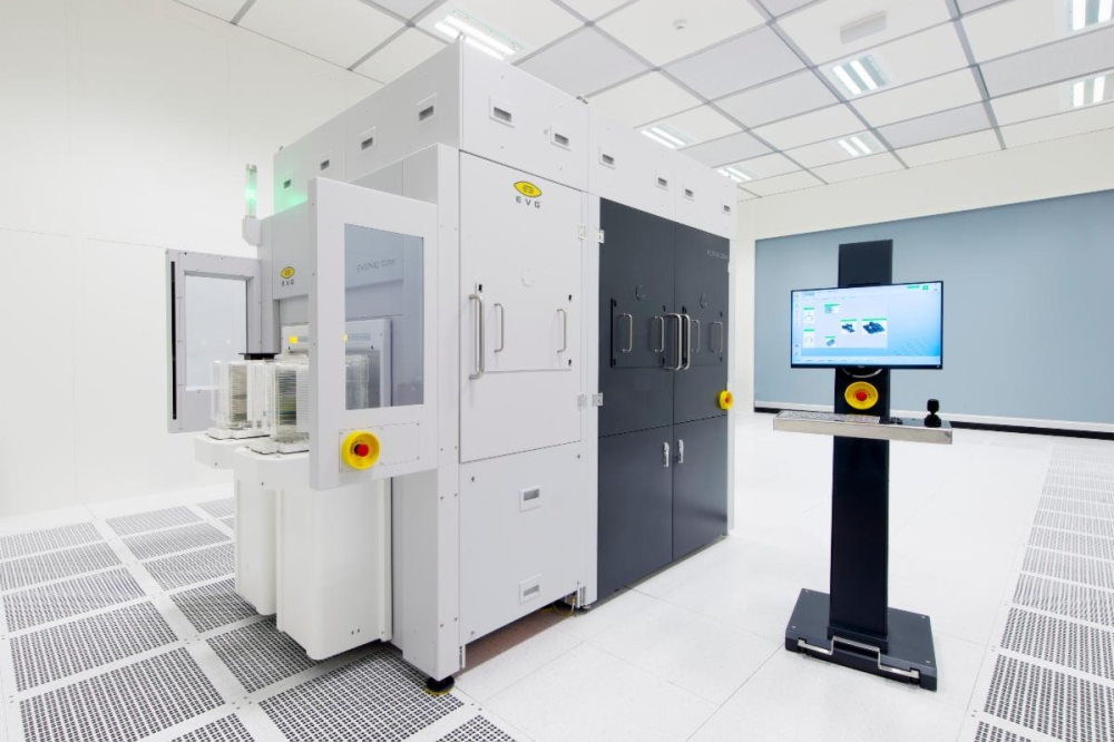
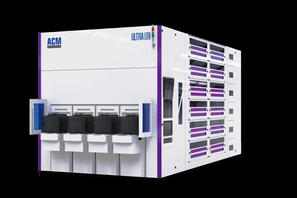
Glass's march from pilot lines to volume hinges less on raw material availability - melting furnaces exist in every region - than on the emerging ecosystem of laser drilling, copper filling, panel handling, and design automation. Yield learning curves, via-fill reliability, panel warpage, and design-kit maturity will determine whether glass meets the cost targets set by system integrators.
Understanding who is installing capacity, which drilling techniques are moving from proof-of-concept to 24/7 production, and how quickly design tools can model gigahertz losses or sub-micron warpage is therefore essential for anyone betting on the timing of adoption.
Equally important is the competitive dynamic with silicon and improved organics. Foundries are pushing hybrid wafer-level redistribution that narrows the feature-size advantage glass holds, while laminate suppliers are developing next-generation ABF cores with lower roughness and better CTE matching. The IDTechEx report benchmarks pros and cons across these materials so readers can see clearly where glass is likely to win, and where it will remain a specialty option.
What the IDTechEx report delivers
"Glass in Semiconductors 2026-2036: Applications, Emerging Technologies, and Market Insights" provides the first bottom-up market model segmented by seven physical product classes, from carrier wafers through to photonic tiles. It quantifies unit demand and revenue year by year, maps announced panel capacity against forecast shipments, and analyzes technology readiness in through-glass via drilling, metallization, and multilayer redistribution.
The study also explains the physics behind glass's electrical and mechanical advantages, outlines the processing challenges that remain, and evaluates the impact of high-frequency RF and photonic integration on total addressable market. Readers will gain a clear picture of how large the opportunity is: US$4.4 billion by 2036.