Asian VCSEL foundries select Eulitha’s lithography tool
Eulitha has recently shipped multiple systems to support the rapidly growing demand for VCSELs used in applications ranging from LiDAR, 3D sensing, data centers, and next-generation optical communications.
Eulitha exhibited at CIOE September 10-12th and presented on ‘Innovative optical lithography for high-resolution patterning in semiconductor laser production’ September 11th. The adoption of Eulitha’s technology marks a strategic shift among manufacturers seeking to meet the increasing need for high-resolution patterning that is cost-competitive, particularly as VCSEL designs become more complex.
Growing VCSEL Demand Drives Need for Scalable Lithography
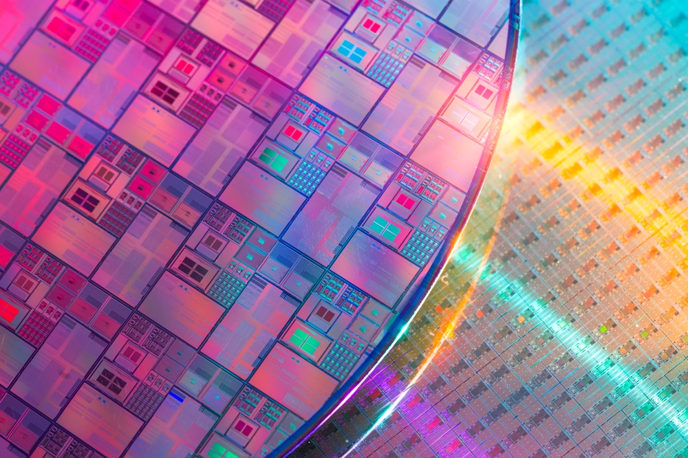
VCSEL technology is experiencing global growth, driven by its pivotal role in enabling high-performance LiDAR systems for autonomous vehicles, 3D facial recognition in consumer electronics, and energy-efficient optical interconnects in data centers. Additionally, polarized sensing—an emerging capability made possible with specially structured VCSELs—offers improved accuracy and contrast in biometric and industrial sensing, fueling further innovation and market expansion.
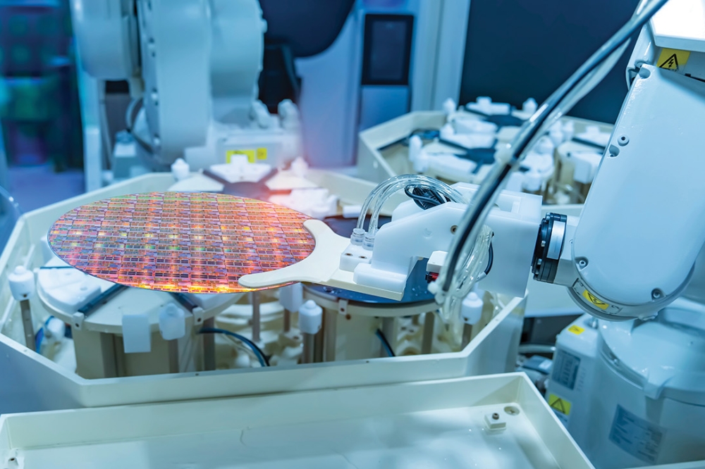
This wave of innovation requires patterning techniques that can deliver extremely high resolution, repeatability, and throughput, cost effectively on 6-inch wafer formats. Eulitha’s technology is uniquely positioned to meet these demands.
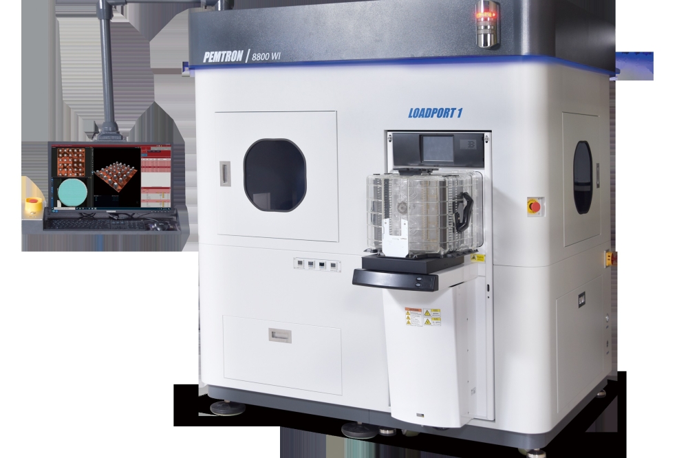
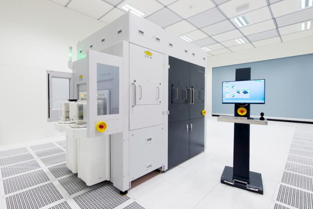
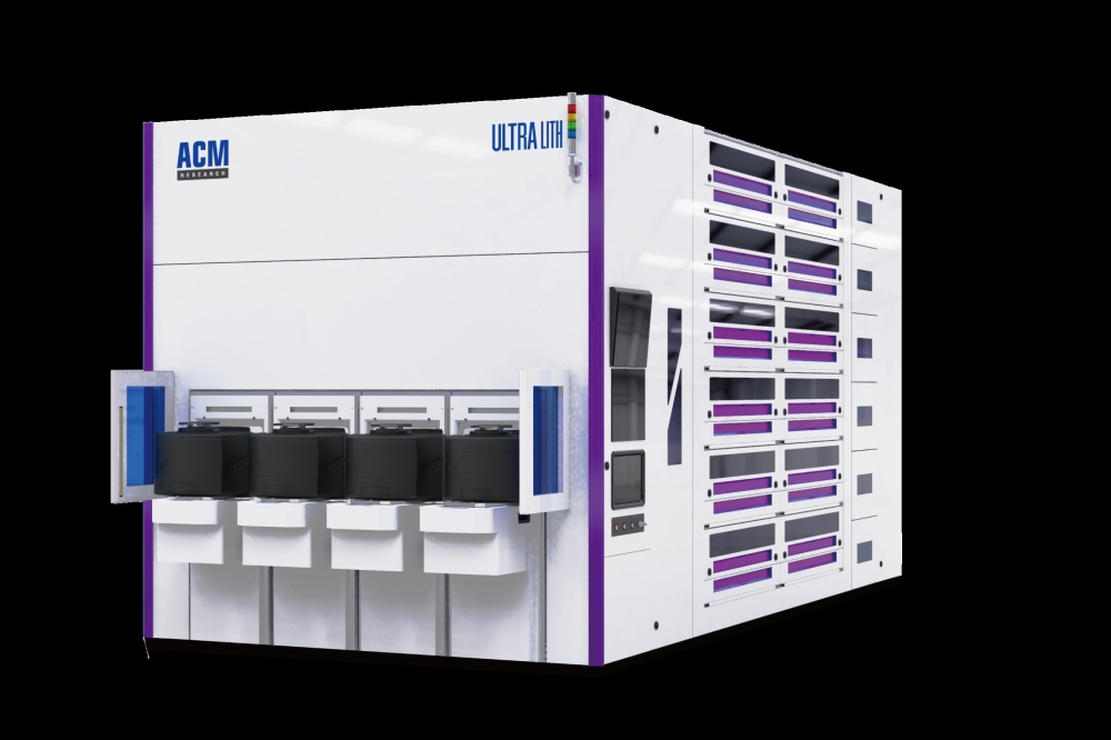
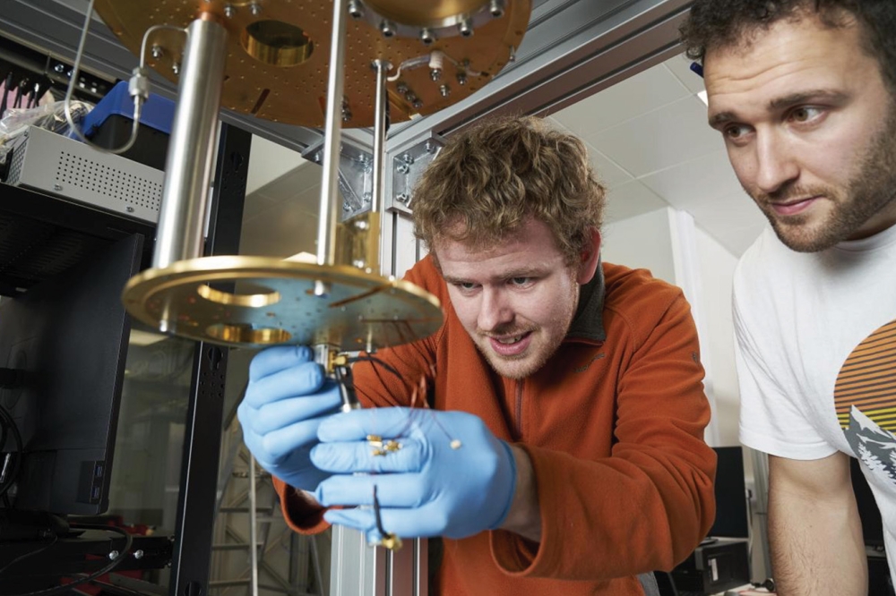
Eulitha’s Lithography
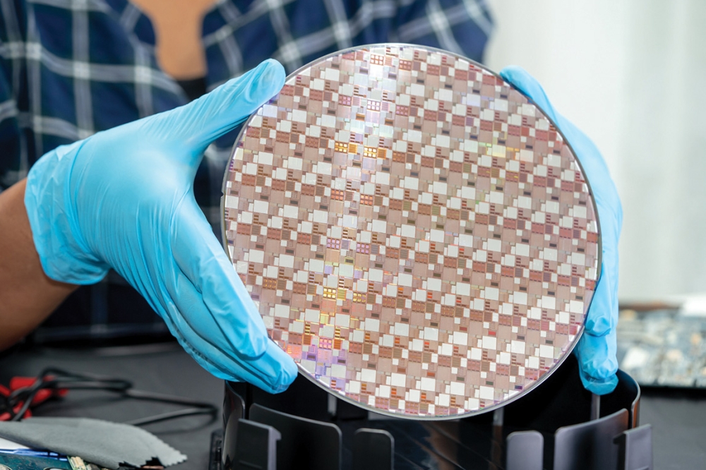
Eulitha’s tool platforms use proprietary non-contact optical lithography technology, known as displacement Talbot lithography (DTL), to deliver a range of advantages. High-resolution, precision patterning is ideal for advanced VCSEL arrays, while its large exposure field covers an entire 6-inch wafer in a single shot, reducing stitching errors and enhancing uniformity. The system supports high-throughput production with consistent results across wafers and production batches. A key feature of DTL is the large depth of focus (DOF), which allows for patterning on non-flat wafers. Together, these capabilities lead to higher device performance, tighter process control, and reduced cost per die for manufacturers.
Supporting the Future of Photonics
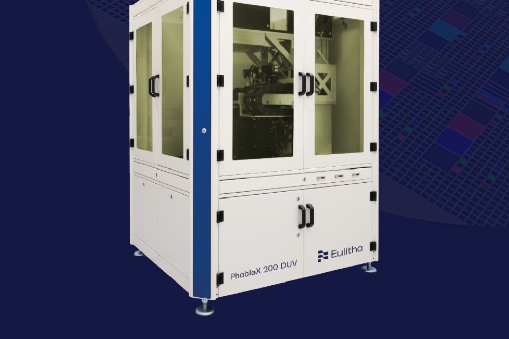
After serving the DFB application market for many years, “VCSEL technology is evolving rapidly, and the market needs lithography tools that can keep up,” said Dr. Harun Solak, CEO of Eulitha. “Our PhableX systems are enabling our customers in Asia to scale up their 6-inch VCSEL production with confidence, delivering the precision and productivity needed to address growing demand in critical sectors like LiDAR and optical interconnects.”
With a growing global customer base and a commitment to delivering precision photonics manufacturing, Eulitha is poised to play a central role in the future of high-performance optoelectronic devices.