Sarcina Technology wins 2026 Best of Show Award at Chiplet Summit
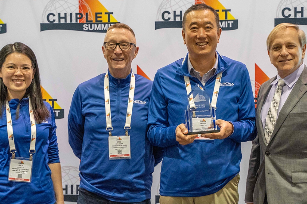
Sarcina Technology, a specialist in semiconductor and photonic packaging, has won the “Packaging: Hardware” category at the 2026 Chiplet Summit Best of Show Awards for its advanced AI package design platform. The award was presented at the fourth annual Chiplet Summit at the Santa Clara Convention Center.
Dr. Larry Zu, CEO at Sarcina Technology comments: “The Sarcina team is delighted to accept this prestigious award for our innovative AI package design platform. Advanced packaging has become the critical enabler of chiplet technology. As AI and high-performance computing drive unprecedented demands for compute density, power delivery and bandwidth, chiplet architectures enabled by advanced packaging are no longer optional, they are the only viable path forward.”
“Sarcina is helping democratize chiplet packaging, enabling startups in communications and AI compute to compete alongside established industry leaders,” said Chuck Sobey, General Chair, Chiplet Summit. “We congratulate them on their innovation and this well-deserved Best of Show recognition.”
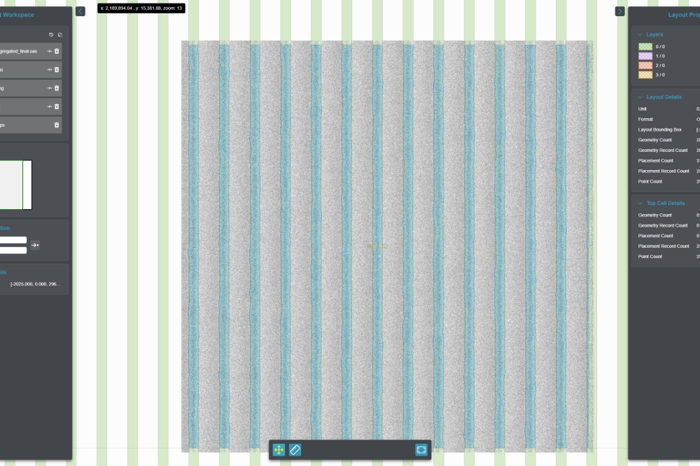
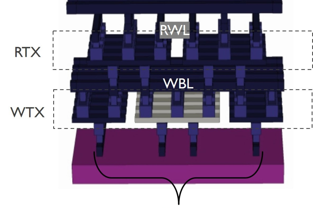
Today’s AI packages may dissipate kilowatts of power, switch hundreds of amperes at high data rates, and must maintain extremely tight power-supply tolerances, all within a highly compact footprint. At the same time, designers must support 100G-plus I/O, dense SerDes and PCIe lanes, HBM integration, LPDDR6 connectivity and UCIe-based die-to-die interconnects operating at 32G and beyond. These requirements push signal integrity, power integrity, thermal and mechanical design to their absolute limits and demand micron-level optimization across complex 2D, 2.5D and 3D heterogeneous package architectures. However, advanced packaging spans far more than interconnect, it also includes novel low-CTE and low-loss substrate materials, ultra-smooth copper, co-packaged optics, photonic IC integration and manufacturable digital twins that predict real-world assembly, yield and cost.
Larry concludes: “At Sarcina, our engineers have embraced the latest semiconductor packaging challenges head-on. Nearly 90 percent of the packages we design now are for AI applications, supporting both compute and data center communications. We are not only designing AI packages based on chiplet architectures, but also leveraging AI to design them. Without AI-driven methodologies, meeting our customers’ aggressive tape-out schedules and performance targets for chiplet-based systems would simply not be possible.”