Gelest collaborates with IBM to test dry resist EUV lithography precursors

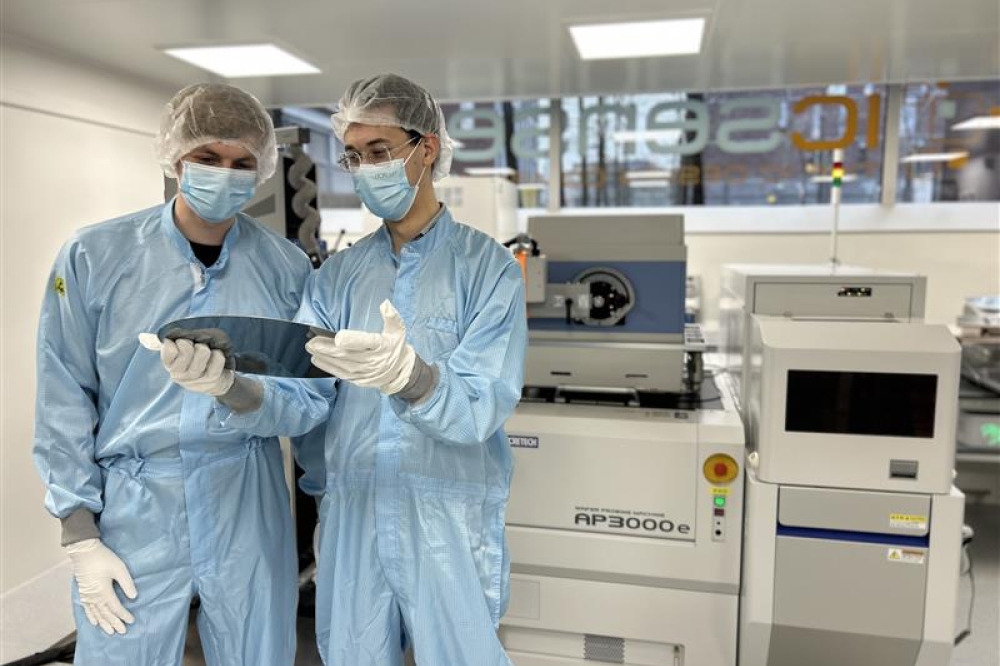
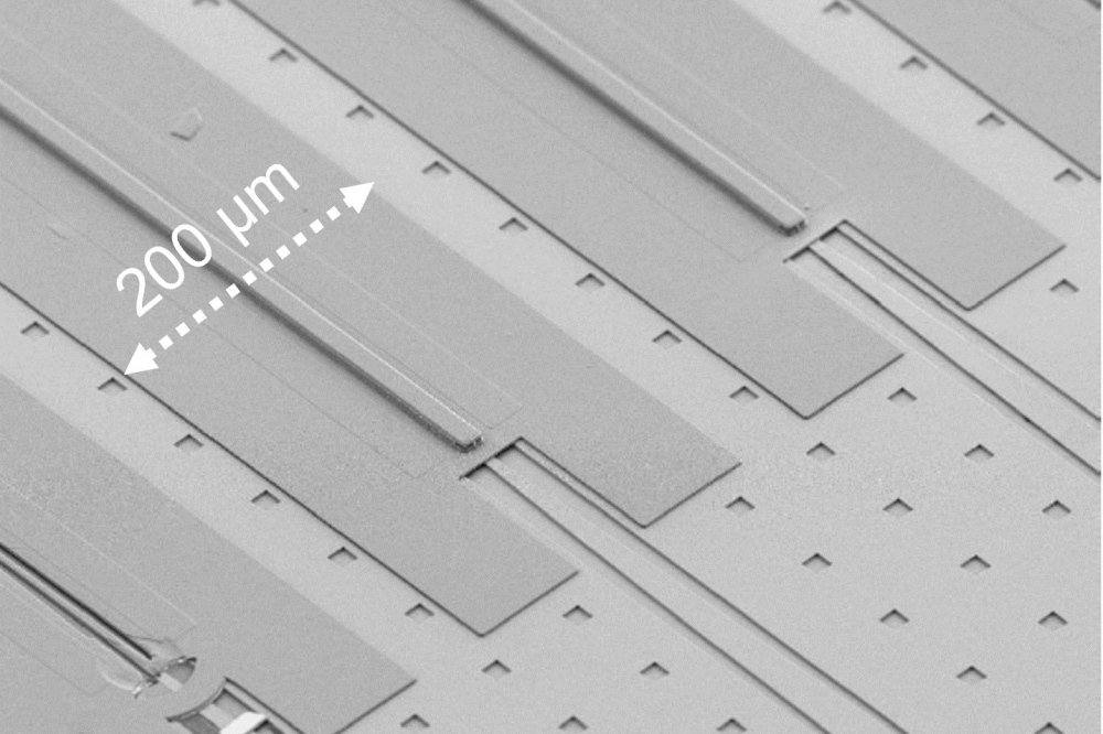
Gelest, Inc., a Mitsubishi Chemical Group company, has formed a research agreement with IBM to test Gelest precursor materials for dry resist EUV lithography. The research collaboration will enable Gelest to see the performance results of its materials for dry resist EUV technology, an advanced semiconductor manufacturing technique driving the next generation of logic and DRAM technologies for the semiconductor market.
“The results of IBM testing will inform the kind of materials we make next,” said Allison Bezden, Gelest global program manager – semiconductor materials. “The collaboration with IBM will aim to speed up innovation cycles and allow Gelest to make data-driven decisions, to make iterations in the lab and to drive the industry forward toward smaller and smaller microelectronic devices.”
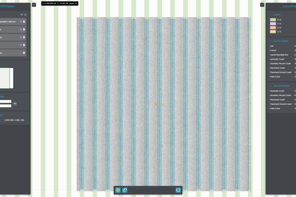
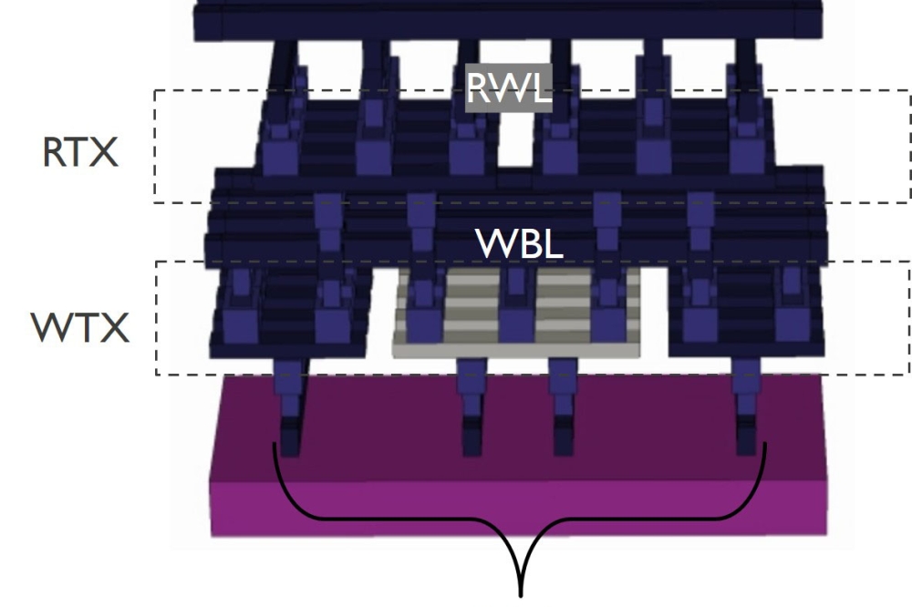
As part of the collaboration, IBM will leverage its baseline EUV process flows and capabilities to evaluate new materials and concepts from Gelest for use in High NA EUV lithography processes.
"We are excited to be working with Gelest as we explore new materials for High NA EUV lithography,” said Huiming Bu, Vice President, IBM Semiconductors Global R&D and Albany Operations, IBM Research. “Collaborations like this are essential to understanding the processes and materials that will support continued scaling to develop smaller, more powerful, and energy-efficient semiconductors needed for the AI era.”
Gelest will share its dry resist precursor expertise by presenting at two upcoming industry events and encourages eventgoers to attend:
Ø Bezden will present, “Redefining EUV lithography: How dry metal oxide resists enable advanced patterning" – at Semicon Korea in Seoul Feb. 12 at 2 pm.
Ø Dr. Li Yang, Ph.D., research and development manager, incubation, will present, “Metal oxide dry resist precursor requirement and advantage towards high-NA EUV lithography” at SPIE Advanced Lithography + Patterning, San Jose, Calif., Feb. 24 at 9:40 am.
In May 2025, Gelest opened a new 50,000-square-foot production facility to increase its production capabilities and support microelectronics and other customer applications, with the main focus on developing and manufacturing precursor chemicals for use in dry resist EUV lithography.