No longer optional: precision sensing for yield improvement in advanced semiconductor manufacturing
How Kistler empowers Semiconductor Equipment Manufacturer for the next era of 3D heterogeneous chip integration
By Robert Hillinger, Kistler Industry Lead Semiconductor
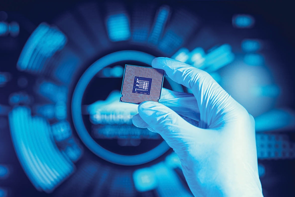
The semiconductor industry has entered a phase in which every micron counts, each defect costs thousands of dollars, and process stability is non-negotiable. From grinding, CMP, thermocompression bonding to advanced testing, machine builders can no longer treat advanced sensing technology as an add-on. Traditionally, MEMS or strain gauge (DMS) sensors were used, but their resolution and stability are no longer sufficient at today’s scale. Integrating high-precision piezoelectric sensor systems, such as those from Kistler, as early as possible in the R&D phase of semiconductor equipment design has become indispensable for meeting the rising demand for yield, quality, and efficiency throughout the machine’s lifecycle.
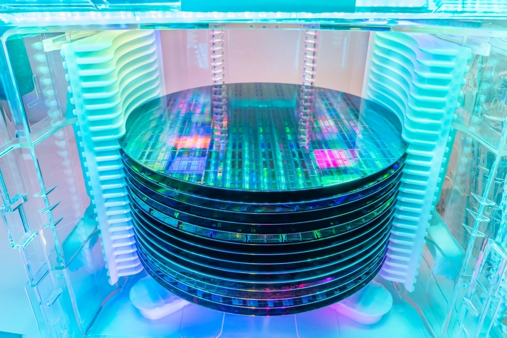
Heterogeneous 3D integration is redefining semiconductor manufacturing by stacking and interconnecting logic, memory, RF, and chiplets into compact, high-performance systems. This technology enables breakthroughs in AI, high-performance computing (HPC), and 5G/6G. However, the complexity of wafer bonding, die stacking, and through-silicon via (TSV) processes poses significant risks. As devices shrink and incorporate fragile new materials, tolerances for force, pressure, vibration, and temperature become critically tight. Yield risks emerge in every step, from alignment in wafer-to-wafer bonding, to void formation in TSV filling, die shift during pick-and-place, and pressure-induced cracks in encapsulation. At the same time, the economic impact of defects increases quickly. Each of the failure modes named above can multiply costs, each worth several thousand dollars apiece.
The conclusion is inevitable for both equipment manufacturers and semiconductor fabs: only machines with built-in, high-precision monitoring and control can ensure process stability, safeguard yield, and protect the massive value tied to every wafer.
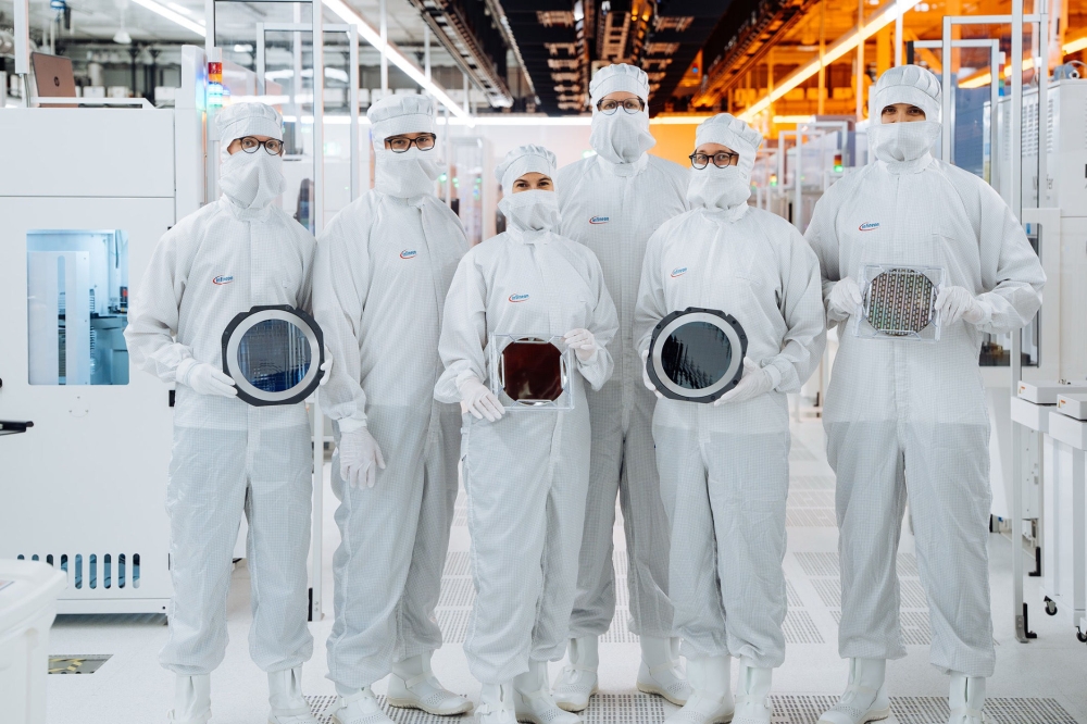
Why semiconductor equipment manufacturer carry the burden of precision
They are at the heart of this transformation, setting industry standards for precision, reliability, and throughput. In the past, success was defined by cycle speed and mechanical accuracy. Today, Semiconductor Manufacturer demand far more, including embedded sensors, closed-loop process control, and traceable quality data that enables predictive maintenance. As a result, machines are evolving from precise mechanical tools into intelligent systems with built-in monitoring and adaptive control.
Failure modes: where yield is put at risk
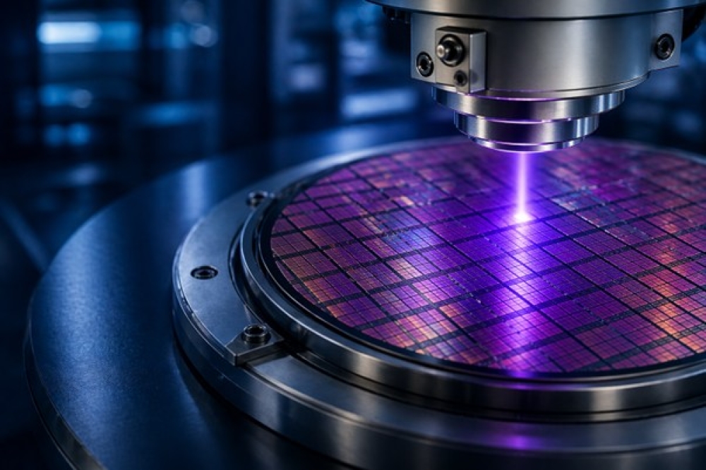
3D integration introduces many different complex and costly failure modes. Methods, such as inline optical inspection, can detect defects, for example, cracks, and misalignment. More damaging risks occur during production and remain invisible to these techniques. Thermal-mechanical stress from coefficient of thermal expansion (CTE) mismatches can cause warpage or micro-cracks. TSV processes are prone to incomplete filling and void formation, which compromise electrical integrity. As well a shift or tilt of a few microns during pick-and-place can disrupt chip alignment and prevent accurate contact matching between interconnect structures, while incorrect pressure during encapsulation can damage fragile dies.
Advanced sensor technologies: the backbone of smart, high-yield 3D integration
High-resolution piezoelectric force sensors integrated directly into bonding heads provide continuous monitoring to help mitigate these risks. Kistler’s sensor portfolio allows Semiconductor Equipment Manufacturer to implement closed-loop control and ensure consistent process transparency. It also provides high resolution with reliable signal integrity data for process optimization and traceability. At the same time, the sensors remain stable and reliable even in high-temperature bonding and encapsulation, and are also suitable for cleanroom and vacuum applications.

Ultra-compact piezoelectric force sensors, such as the Type 9172CD from Kistler, measure micro-forces ranging from sub-newton to kilonewton, providing high-resolution, real-time data directly from critical process points. This helps manufacturers prevent failures such as die shift, and pressure-induced microcracks
Compact, high-sensitivity force sensors cover ranges from nanonewton to kilonewton, supporting applications from precise grinding, CMP, bonding to chiplet placement and packaging. By detecting micro-forces in real time, these sensors enable precise process control at bonding points, minimize the risk of die damage, and maintain stability even at high throughput. As placement heads accelerate and decelerate, Acceleration sensors track micro-vibrations and shocks that can shift dies by mere microns. When the process continues into encapsulation, underfill, or TSV filling, next-generation pressure sensors provide real-time cavity monitoring to detect voids, maintain uniform fill, and secure stable process conditions.
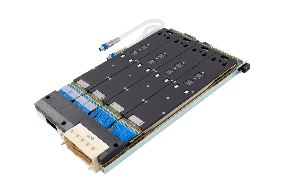
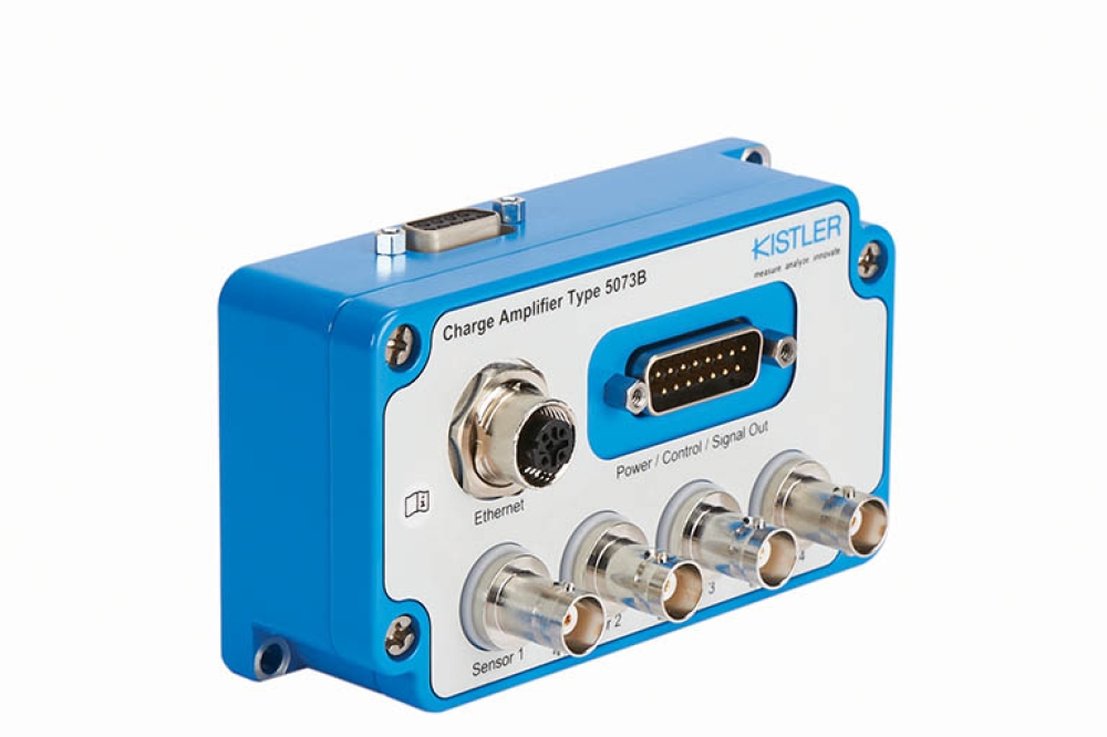
To tie these signals together, the industrial charge amplifier delivers force monitoring with real-time signals for the Semiconductor Equipment control system. Designed for multipurpose use with piezoelectric sensors, the Amplifier converts charge signals from sensors into voltage and/or digital outputs. This closed-loop control system ensures precise bonding alignment and prevents defects caused by overpressure. Additionally, handheld diagnostic tools with integrated charge amplifiers enable engineers to validate process parameter verification and quality control processes anywhere.
Sensor placement: there is no one-size-fits-all solution
Designing equipment for heterogeneous 3D integration means more than simply selecting the appropriate sensing technology. It also requires placing sensors exactly where they deliver maximum insight. The ideal measurement location may not offer the environmental conditions needed for long sensor life. For example, while piezoelectric sensors can tolerate high temperatures, they still have operational limits. In certain applications, it may be necessary to use a more heat-resistant sensor or adjust the placement to ensure equipment protection and reliability.

The new Miniature Triaxial Acceleration sensor Z22198 from Kistler is designed for high-precision vibration analysis, including micro-vibrations and shocks. The lightweight miniature Sensor is ideal for dynamics testing and monitoring, especially in tight spaces
Kistler works closely with Semiconductor Equipment Manufacturer to identify the most sensitive points within their systems, ensuring that force, pressure, and vibration sensors are embedded where they capture the most informative data. Further services such as calibration, and system validation during equipment build, ensure long-term accuracy and reliability.
Taking bold action: securing yield and strategic advantage in 3D integration
Delaying investments in advanced sensor systems and smart manufacturing technologies presents risks for Semiconductor Equipment Manufacturer. As product requirements evolve – such as miniaturization or the use of new materials – process stability can be compromised. Retrofitting sensors into completed machines is often technically challenging. Space constraints and even minor modifications can disrupt process balance or amplify existing issues. Even, when possible, retrofits rarely match the performance of solutions integrated during the design phase. Looking ahead, more sophisticated – and expensive – wafer materials, like Gallium Nitride and Siliciumcarbid, and the further advancement of manufacturing processes will only increase the need for better monitoring strategies. High-resolution sensors will become even more central to securing long-term competitiveness.